'%20fill='%23ea002c'/%3e%3cpath%20d='M31.44,109.48l7.92-9.71H33.72l-6.32,8.38h-.1V99.77H22.65v20.58h.28c2,0,4.4-.93,4.4-4.29v-4.73h.1l6.44,8.76h5.92Z'%20transform='translate(-5.29%20-72.33)'%20fill='%23ea002c'/%3e%3c/g%3e%3cg%3e%3cpath%20d='M39.63,77.72c-1.64.31-4.07,1.8-4.06,4.43,0,2.39,2,3.83,2,7a5.54,5.54,0,0,1-2.69,4.82c.57-.05,1.19-.08,1.87-.08a14.65,14.65,0,0,1,2.35.14l7.35-9A30.51,30.51,0,0,0,39.63,77.72Z'%20transform='translate(-5.29%20-72.33)'%20fill='%23ea002c'/%3e%3cpath%20d='M45.8,102.08c.93-1.44,1-3.74,1.12-6.07s.55-3.83,3.46-3.84c.65,0,1.26.09,2.38.09a17.2,17.2,0,0,0,8.8-2.46A30.54,30.54,0,0,0,46.41,85c-.41,1.18-3.67,10.23-3.92,11a11.32,11.32,0,0,1,1.32,1.93A21.12,21.12,0,0,1,45.8,102.08Z'%20transform='translate(-5.29%20-72.33)'%20fill='%23ea002c'/%3e%3cpath%20d='M30.28,94.69c-.38,0-.56-.25-.61-.68s-1.89-17.24-2.16-19.79c0-.37-.13-1-.13-1.3a.53.53,0,0,1,.55-.59c.87,0,5.62,1.11,10.66,4.64a5.37,5.37,0,0,0-4.07,5c0,2.77,2,4.29,2,7.07C36.54,93.59,31.35,94.69,30.28,94.69Z'%20transform='translate(-5.29%20-72.33)'%20fill='%23ff7a00'/%3e%3cpath%20d='M46.22,103.28a3.7,3.7,0,0,0,.23.51.52.52,0,0,0,.45.28,1.09,1.09,0,0,0,.42-.11l18.06-8.39c.33-.16,1-.45,1.18-.57a.56.56,0,0,0,.31-.49.58.58,0,0,0-.09-.3,18.5,18.5,0,0,0-4.25-3.76,19.07,19.07,0,0,1-9.63,2.78c-1.12,0-1.38-.08-2.14-.07-2.24,0-2.8,1-2.88,2.92,0,.37,0,.87,0,1.42C47.77,99.25,47.56,101.66,46.22,103.28Z'%20transform='translate(-5.29%20-72.33)'%20fill='%23ff7a00'/%3e%3c/g%3e%3cg%3e%3cpath%20d='M70.2,120.63c-1.7,4.61-3.89,5.2-5.78,5.2A5.55,5.55,0,0,1,62,125.3l.71-2.15a3.69,3.69,0,0,0,1.58.42c1.49,0,2.43-.84,3.26-3.44l-5.14-11.21a5.45,5.45,0,0,1,1.39-.21c1.65,0,2,1,2.43,2.06.36.85,2.7,6.51,2.7,6.51H69l2.72-8.36h2.81Z'%20transform='translate(-5.29%20-72.33)'%20fill='%23ff7a00'/%3e%3cpath%20d='M107.43,120.08l-3.93-5.72,3.85-5.6H104l-2.68,4.1-1.61-2.53c-.54-.83-1-1.66-2.25-1.63a2.46,2.46,0,0,0-.52,0,4.83,4.83,0,0,0-1.33.47c0,.06,1.89,2.68,3.65,5.22l-3.88,5.64h3.32l2.7-4.12,2.69,4.12Z'%20transform='translate(-5.29%20-72.33)'%20fill='%23ff7a00'/%3e%3cpath%20d='M76.84,112.6v7.49h2.81V112.3a3.79,3.79,0,0,1,2.26-1.09,2.16,2.16,0,0,1,2.2,2.41v6.47h2.81v-7.17a3.87,3.87,0,0,0-4.08-4.16,5.09,5.09,0,0,0-3.39,1.47A1.81,1.81,0,0,0,77.57,109a5.79,5.79,0,0,0-1,.14A14.85,14.85,0,0,1,76.84,112.6Z'%20transform='translate(-5.29%20-72.33)'%20fill='%23ff7a00'/%3e%3cg%3e%3cpath%20d='M93.2,105.54a1.74,1.74,0,1,1-1.74-1.69A1.71,1.71,0,0,1,93.2,105.54Z'%20transform='translate(-5.29%20-72.33)'%20fill='%23ff7a00'/%3e%3crect%20x='84.78'%20y='36.59'%20width='2.79'%20height='11.16'%20fill='%23ff7a00'/%3e%3c/g%3e%3cpath%20d='M53.44,110.2a5.74,5.74,0,0,1,3.62-1.49c2.19,0,3.8,1.14,3.8,3.91v7.47H57.94v-6.67a2,2,0,0,0-2-2.18,4.24,4.24,0,0,0-2.54,1.21v7.64h-2.9v-17h.62a2.22,2.22,0,0,1,2.28,2.35Z'%20transform='translate(-5.29%20-72.33)'%20fill='%23ff7a00'/%3e%3c/g%3e%3c/g%3e%3c/svg%3e)
Advanced Memory Package Architecture
Advanced Memory Package Architecture is a research domain dedicated to developing package structures, stacking methodologies, interconnects, thermal management solutions, and reliability technologies for next-generation high-performance memory. This field addresses the growing demand for memory with high storage capacity and low latency, critical for system performance in AI, HPC, data centers, and high-end GPU/ASIC markets. Technologies such as HB (High Bandwidth) Memory, HBM (Memory Package), and HBF (stacked memory) are becoming increasingly vital, surpassing traditional DDR/LPDDR-centric architectures. The core focus of this research area extends beyond simply stacking memory chips; it aims to simultaneously optimize bandwidth, capacity, thermal characteristics, stack height, TSV (Through-Silicon Via) density, bonding pitch, and package reliability. Furthermore, to achieve diverse market needs ranging from mobile to server and new AI architectures, the research actively develops the VFO (Vertical Fan-Out) platform. VFO is defined as a cost-effective alternative to TSV-based stacking. It achieves significant form factor reduction, surpassing the limits of conventional wire-bonding, and provides a scalable, optimized memory solution for all AI market segments.
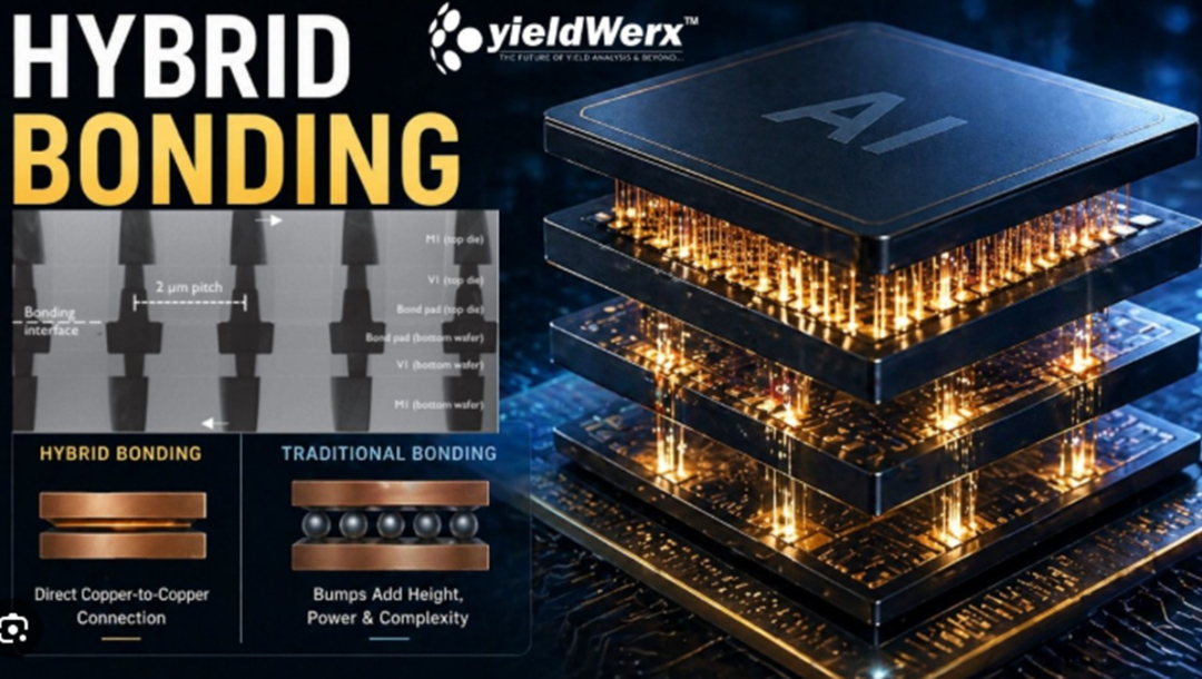
Next-Generation HBM Package Architecture
- Increasing the number of stacked layers in HBM stacks.
- Scaling TSV pitch and TSV density.
- Transitioning from micro-bump-based structures to hybrid bonding-based structures.
- Optimizing the functionality of the HBM base die for logic layer die.
- Designing the stacking, thermal dissipation, and heat paths considering heat dissipation.
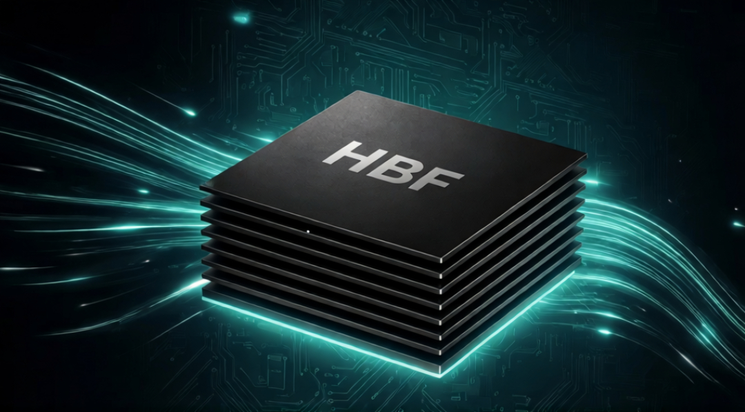
HBF Memory Package Architecture
- Designing the optimal stacking structure for HBF memory stacks.
- Researching vertical interconnect architectures between HBF dies.
- Analyzing package-level signal integrity and power integrity.
- Researching multi-stack architectures for increased capacity.
- Analyzing thermal bottlenecks in HBF packages and designing cooling paths.
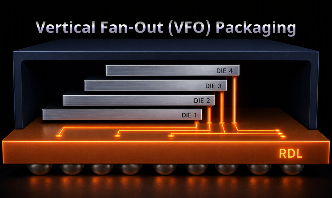
Scalable Memory Package Architecture
- Developing optimized VFO solutions for Mobile, Server, and New AI Architecture markets.
- Implementing TSV-less high-density vertical interconnects to maximize bandwidth and capacity with cost efficiency.
- Designing advanced package structures that minimize footprint and enhance signal integrity for on-device AI.
- Validating ultra-thin multi-die stacking (e.g., 8-high) and thermal reliability for high-density packages.
Want to learn more about how we can create new values for semiconductor industry? Please contact us!
We are in this together! Contact Us