'%20fill='%23ea002c'/%3e%3cpath%20d='M31.44,109.48l7.92-9.71H33.72l-6.32,8.38h-.1V99.77H22.65v20.58h.28c2,0,4.4-.93,4.4-4.29v-4.73h.1l6.44,8.76h5.92Z'%20transform='translate(-5.29%20-72.33)'%20fill='%23ea002c'/%3e%3c/g%3e%3cg%3e%3cpath%20d='M39.63,77.72c-1.64.31-4.07,1.8-4.06,4.43,0,2.39,2,3.83,2,7a5.54,5.54,0,0,1-2.69,4.82c.57-.05,1.19-.08,1.87-.08a14.65,14.65,0,0,1,2.35.14l7.35-9A30.51,30.51,0,0,0,39.63,77.72Z'%20transform='translate(-5.29%20-72.33)'%20fill='%23ea002c'/%3e%3cpath%20d='M45.8,102.08c.93-1.44,1-3.74,1.12-6.07s.55-3.83,3.46-3.84c.65,0,1.26.09,2.38.09a17.2,17.2,0,0,0,8.8-2.46A30.54,30.54,0,0,0,46.41,85c-.41,1.18-3.67,10.23-3.92,11a11.32,11.32,0,0,1,1.32,1.93A21.12,21.12,0,0,1,45.8,102.08Z'%20transform='translate(-5.29%20-72.33)'%20fill='%23ea002c'/%3e%3cpath%20d='M30.28,94.69c-.38,0-.56-.25-.61-.68s-1.89-17.24-2.16-19.79c0-.37-.13-1-.13-1.3a.53.53,0,0,1,.55-.59c.87,0,5.62,1.11,10.66,4.64a5.37,5.37,0,0,0-4.07,5c0,2.77,2,4.29,2,7.07C36.54,93.59,31.35,94.69,30.28,94.69Z'%20transform='translate(-5.29%20-72.33)'%20fill='%23ff7a00'/%3e%3cpath%20d='M46.22,103.28a3.7,3.7,0,0,0,.23.51.52.52,0,0,0,.45.28,1.09,1.09,0,0,0,.42-.11l18.06-8.39c.33-.16,1-.45,1.18-.57a.56.56,0,0,0,.31-.49.58.58,0,0,0-.09-.3,18.5,18.5,0,0,0-4.25-3.76,19.07,19.07,0,0,1-9.63,2.78c-1.12,0-1.38-.08-2.14-.07-2.24,0-2.8,1-2.88,2.92,0,.37,0,.87,0,1.42C47.77,99.25,47.56,101.66,46.22,103.28Z'%20transform='translate(-5.29%20-72.33)'%20fill='%23ff7a00'/%3e%3c/g%3e%3cg%3e%3cpath%20d='M70.2,120.63c-1.7,4.61-3.89,5.2-5.78,5.2A5.55,5.55,0,0,1,62,125.3l.71-2.15a3.69,3.69,0,0,0,1.58.42c1.49,0,2.43-.84,3.26-3.44l-5.14-11.21a5.45,5.45,0,0,1,1.39-.21c1.65,0,2,1,2.43,2.06.36.85,2.7,6.51,2.7,6.51H69l2.72-8.36h2.81Z'%20transform='translate(-5.29%20-72.33)'%20fill='%23ff7a00'/%3e%3cpath%20d='M107.43,120.08l-3.93-5.72,3.85-5.6H104l-2.68,4.1-1.61-2.53c-.54-.83-1-1.66-2.25-1.63a2.46,2.46,0,0,0-.52,0,4.83,4.83,0,0,0-1.33.47c0,.06,1.89,2.68,3.65,5.22l-3.88,5.64h3.32l2.7-4.12,2.69,4.12Z'%20transform='translate(-5.29%20-72.33)'%20fill='%23ff7a00'/%3e%3cpath%20d='M76.84,112.6v7.49h2.81V112.3a3.79,3.79,0,0,1,2.26-1.09,2.16,2.16,0,0,1,2.2,2.41v6.47h2.81v-7.17a3.87,3.87,0,0,0-4.08-4.16,5.09,5.09,0,0,0-3.39,1.47A1.81,1.81,0,0,0,77.57,109a5.79,5.79,0,0,0-1,.14A14.85,14.85,0,0,1,76.84,112.6Z'%20transform='translate(-5.29%20-72.33)'%20fill='%23ff7a00'/%3e%3cg%3e%3cpath%20d='M93.2,105.54a1.74,1.74,0,1,1-1.74-1.69A1.71,1.71,0,0,1,93.2,105.54Z'%20transform='translate(-5.29%20-72.33)'%20fill='%23ff7a00'/%3e%3crect%20x='84.78'%20y='36.59'%20width='2.79'%20height='11.16'%20fill='%23ff7a00'/%3e%3c/g%3e%3cpath%20d='M53.44,110.2a5.74,5.74,0,0,1,3.62-1.49c2.19,0,3.8,1.14,3.8,3.91v7.47H57.94v-6.67a2,2,0,0,0-2-2.18,4.24,4.24,0,0,0-2.54,1.21v7.64h-2.9v-17h.62a2.22,2.22,0,0,1,2.28,2.35Z'%20transform='translate(-5.29%20-72.33)'%20fill='%23ff7a00'/%3e%3c/g%3e%3c/g%3e%3c/svg%3e)
Heterogeneous Integration Package Technology
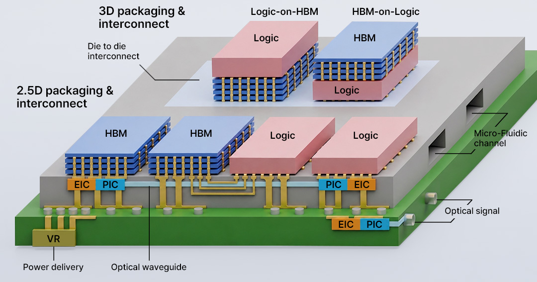
Heterogeneous Integration Package Technology is a next-generation semiconductor packaging technology that integrates various semiconductor dies or chiplets with different functions, process nodes, sizes, materials, and performance characteristics into a single package. At the core lies new and technical limitations of fine-pitch scaling intensity, the importance of heterogeneous integration—connecting functionally optimized chiplets at the package level with high density—is rapidly growing compared to the traditional approach of integrating all functions into a single monolithic SoC.
This research area encompasses 2.5D package platforms, 3D package platforms, chiplet architecture, die-to-die interfaces, and high-density redistribution layers (RDL). The ultimate goal is to implement a next-generation system package platform that simultaneously satisfies high performance, low power consumption, high yield, and high scalability.
Particularly in high-performance computing systems such as AI accelerators, HPC processors, high-end GPUs, network processors, and edge AI devices, computational performance, memory bandwidth, power efficiency, and I/O scalability have emerged as key competitive factors. Consequently, heterogeneous integration packages are establishing themselves as the core technology platform determining system performance.
2.5D Package Platform
- Research on high-density routing architecture based on silicon interposers
- Research on embedded silicon bridge structures
- Optimization of high-bandwidth connections between HBM and logic dies
3D Package Platform
- Research on memory-on-logic 3D stacking
- Research on homogenous 3D integration based on hybrid bonding
- Research on face-to-face and face-to-back bonding architectures
- Research on thermal-aware 3D floorplanning
Want to learn more about how we can create new values for semiconductor industry? Please contact us!
We are in this together! Contact Us