'%20fill='%23ea002c'/%3e%3cpath%20d='M31.44,109.48l7.92-9.71H33.72l-6.32,8.38h-.1V99.77H22.65v20.58h.28c2,0,4.4-.93,4.4-4.29v-4.73h.1l6.44,8.76h5.92Z'%20transform='translate(-5.29%20-72.33)'%20fill='%23ea002c'/%3e%3c/g%3e%3cg%3e%3cpath%20d='M39.63,77.72c-1.64.31-4.07,1.8-4.06,4.43,0,2.39,2,3.83,2,7a5.54,5.54,0,0,1-2.69,4.82c.57-.05,1.19-.08,1.87-.08a14.65,14.65,0,0,1,2.35.14l7.35-9A30.51,30.51,0,0,0,39.63,77.72Z'%20transform='translate(-5.29%20-72.33)'%20fill='%23ea002c'/%3e%3cpath%20d='M45.8,102.08c.93-1.44,1-3.74,1.12-6.07s.55-3.83,3.46-3.84c.65,0,1.26.09,2.38.09a17.2,17.2,0,0,0,8.8-2.46A30.54,30.54,0,0,0,46.41,85c-.41,1.18-3.67,10.23-3.92,11a11.32,11.32,0,0,1,1.32,1.93A21.12,21.12,0,0,1,45.8,102.08Z'%20transform='translate(-5.29%20-72.33)'%20fill='%23ea002c'/%3e%3cpath%20d='M30.28,94.69c-.38,0-.56-.25-.61-.68s-1.89-17.24-2.16-19.79c0-.37-.13-1-.13-1.3a.53.53,0,0,1,.55-.59c.87,0,5.62,1.11,10.66,4.64a5.37,5.37,0,0,0-4.07,5c0,2.77,2,4.29,2,7.07C36.54,93.59,31.35,94.69,30.28,94.69Z'%20transform='translate(-5.29%20-72.33)'%20fill='%23ff7a00'/%3e%3cpath%20d='M46.22,103.28a3.7,3.7,0,0,0,.23.51.52.52,0,0,0,.45.28,1.09,1.09,0,0,0,.42-.11l18.06-8.39c.33-.16,1-.45,1.18-.57a.56.56,0,0,0,.31-.49.58.58,0,0,0-.09-.3,18.5,18.5,0,0,0-4.25-3.76,19.07,19.07,0,0,1-9.63,2.78c-1.12,0-1.38-.08-2.14-.07-2.24,0-2.8,1-2.88,2.92,0,.37,0,.87,0,1.42C47.77,99.25,47.56,101.66,46.22,103.28Z'%20transform='translate(-5.29%20-72.33)'%20fill='%23ff7a00'/%3e%3c/g%3e%3cg%3e%3cpath%20d='M70.2,120.63c-1.7,4.61-3.89,5.2-5.78,5.2A5.55,5.55,0,0,1,62,125.3l.71-2.15a3.69,3.69,0,0,0,1.58.42c1.49,0,2.43-.84,3.26-3.44l-5.14-11.21a5.45,5.45,0,0,1,1.39-.21c1.65,0,2,1,2.43,2.06.36.85,2.7,6.51,2.7,6.51H69l2.72-8.36h2.81Z'%20transform='translate(-5.29%20-72.33)'%20fill='%23ff7a00'/%3e%3cpath%20d='M107.43,120.08l-3.93-5.72,3.85-5.6H104l-2.68,4.1-1.61-2.53c-.54-.83-1-1.66-2.25-1.63a2.46,2.46,0,0,0-.52,0,4.83,4.83,0,0,0-1.33.47c0,.06,1.89,2.68,3.65,5.22l-3.88,5.64h3.32l2.7-4.12,2.69,4.12Z'%20transform='translate(-5.29%20-72.33)'%20fill='%23ff7a00'/%3e%3cpath%20d='M76.84,112.6v7.49h2.81V112.3a3.79,3.79,0,0,1,2.26-1.09,2.16,2.16,0,0,1,2.2,2.41v6.47h2.81v-7.17a3.87,3.87,0,0,0-4.08-4.16,5.09,5.09,0,0,0-3.39,1.47A1.81,1.81,0,0,0,77.57,109a5.79,5.79,0,0,0-1,.14A14.85,14.85,0,0,1,76.84,112.6Z'%20transform='translate(-5.29%20-72.33)'%20fill='%23ff7a00'/%3e%3cg%3e%3cpath%20d='M93.2,105.54a1.74,1.74,0,1,1-1.74-1.69A1.71,1.71,0,0,1,93.2,105.54Z'%20transform='translate(-5.29%20-72.33)'%20fill='%23ff7a00'/%3e%3crect%20x='84.78'%20y='36.59'%20width='2.79'%20height='11.16'%20fill='%23ff7a00'/%3e%3c/g%3e%3cpath%20d='M53.44,110.2a5.74,5.74,0,0,1,3.62-1.49c2.19,0,3.8,1.14,3.8,3.91v7.47H57.94v-6.67a2,2,0,0,0-2-2.18,4.24,4.24,0,0,0-2.54,1.21v7.64h-2.9v-17h.62a2.22,2.22,0,0,1,2.28,2.35Z'%20transform='translate(-5.29%20-72.33)'%20fill='%23ff7a00'/%3e%3c/g%3e%3c/g%3e%3c/svg%3e)
Next Generation Materials
Memory technology is moving past the limits of two-dimensional scaling and into the vertical dimension: DRAM is building upward and NAND continues pushing toward ever-higher stacks, and amid the AI-driven demand for high-performance memory, the importance of wafer-level-package (WLP) materials has grown substantially in securing HBM device performance and reliability. The vertical era pushes aspect ratios to extremes and in the packaging domain it demands far more precise planarization. To meet the performance that devices demand, material innovation of an entirely new concept and even more precise control are required. Realizing ultra-fine patterning and three-dimensional structures now hinges on material technology that tunes the chemical and physical properties of key process materials at the molecular scale. EUV materials for ultra-fine patterning require development of new photoresist chemistries to overcome the increasingly tight RLS trade-off. Etch gases hold the profile fidelity of high-aspect-ratio patterns, precursors drive uniform films and defect suppression, chemicals and CMP slurries set planarization precision, and wafers anchor the substrate yield that everything else builds on. When molecular-scale design and ultra-high-purity purification deliver angstrom-scale control, competitiveness in next-generation semiconductor manufacturing moves beyond a reliance on equipment performance alone and into a structure where material technology holds the lead. Our research converges over one direction — total material solutions that span patterning, chemicals, CMP, etch gases, precursors, and wafers, turning each of these challenges into the next generation of memory and storage.
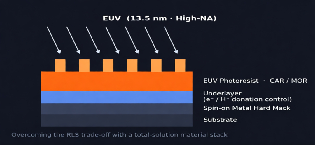
Patterning Materials - EUV Total Solution
- Toward shorter wavelengths, higher NA, and multi-patterning, we develop a complete EUV material stack that overcomes the resolution-LER-sensitivity (RLS) trade-off while maximizing productivity.
- CAR: low-LUMO polymers optimized with high-absorption PAGs to advance chemically amplified resists.
- MOR: a new approach built on multi-ligand design and high-EUV-absorption metal cores.
- Pattern-assist: pattern-expansion materials and underlayers controlling secondary-electron and H⁺ donation.
- Overcome resolution limits, we develop next level materials: molecular-level resists & spin-on metal hard mask
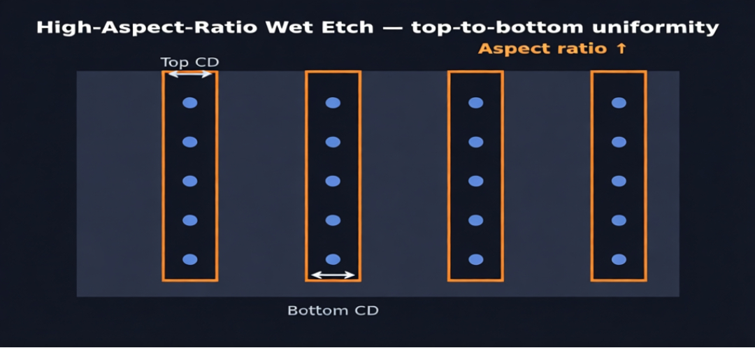
Chemical Materials - Precision Wet-Etch Chemistry
- As DRAM and NAND stack up, key etch steps shift from dry to wet: metal-recess control and top-to-bottom uniformity across extreme aspect ratios are now the core of etch technology.
- Maximized etch selectivity that removes only the intended film deep inside high-aspect-ratio structures.
- Etch-rate-controllable raw materials balancing etch-enhancing and etch-inhibiting functions for uniform removal.
- Etch by-product solubility enhancement : Materials that maximize the solubility of by-products generated during wet etching to ensure yield and integrity.
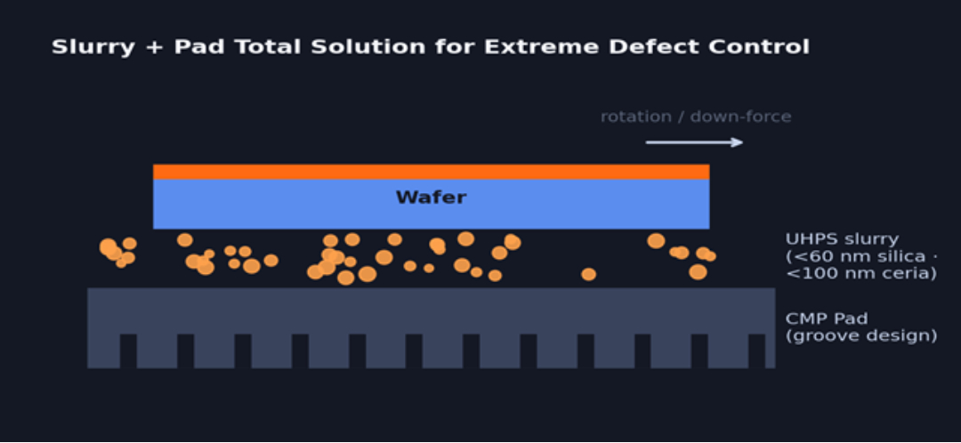
CMP Materials - Ultra-High Planarization & Defect controllability
- Pitch-down and stack-up multiply CMP steps and make extreme defect control a core process technology: slurry and pad are co-optimized as one total solution.
- UHPS transition: abrasive engineering with sub-60 nm colloidal silica and sub-100 nm ceria particles.
- Charge-controlling additives for stable abrasive dispersion and minimal defectivity.
- Pad groove material and shape optimization, building a total slurry + pad line-up covering diverse substrates.
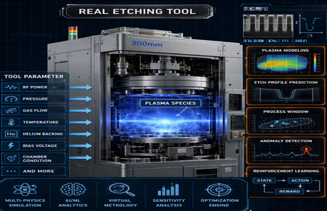
Etch Materials - Etch force control to maximize Aspect Ratio
- Development of an etch gas in which, as part of understanding process physics, gas enters, plasma forms, etching behavior occurs, and chemical reactions proceed smoothly.
- Development of gas with enhanced cleaning efficiency by understanding the dry etching process and by gas flux/atomic ratio
- Physical etching by ion collision as part of the selectivity control mechanism for HARC etch. Prevention of lateral erosion outside the downward vertical ion collision zone for sidewall protection, enabling a perfect vertically isotropic profile; and scavenging effect of the hydrogenation gas
- Low GWP Gas, Cryo Etch Gas Devolope & E/R, Selectivity, Cleaning Efficiency, Particle Control.
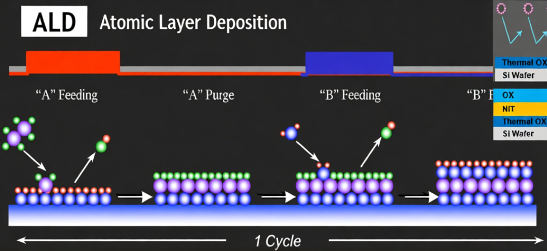
Diffusion Materials - Next-Generation Material Development and Atomic-Stratum-Size Micro-Deposition
- Enhancing thin-film properties through atomic-layer-scale ultra-fine deposition based on the single-type & ALD furnace process
- Development of materials for increasing capacitance and preventing electrode oxidation through the design of optimal combinations of reactants and precursors for high-k oxides
- Early Identification of Novel Materials to Secure the Operational Characteristics of the ICL (Interface Control Layer)
- Optimization of process performance customization and material design capabilities for SIN, SiO, Poly, and Mo implementations
- Material Properties(TGA/DSC/NMR Assay/ Viscosity/Vapor Pressure) & Film Quality(ALD Window, D/R & Unif), Step Coverage, Gap Fill, Loading Effect) & Electrical Performance
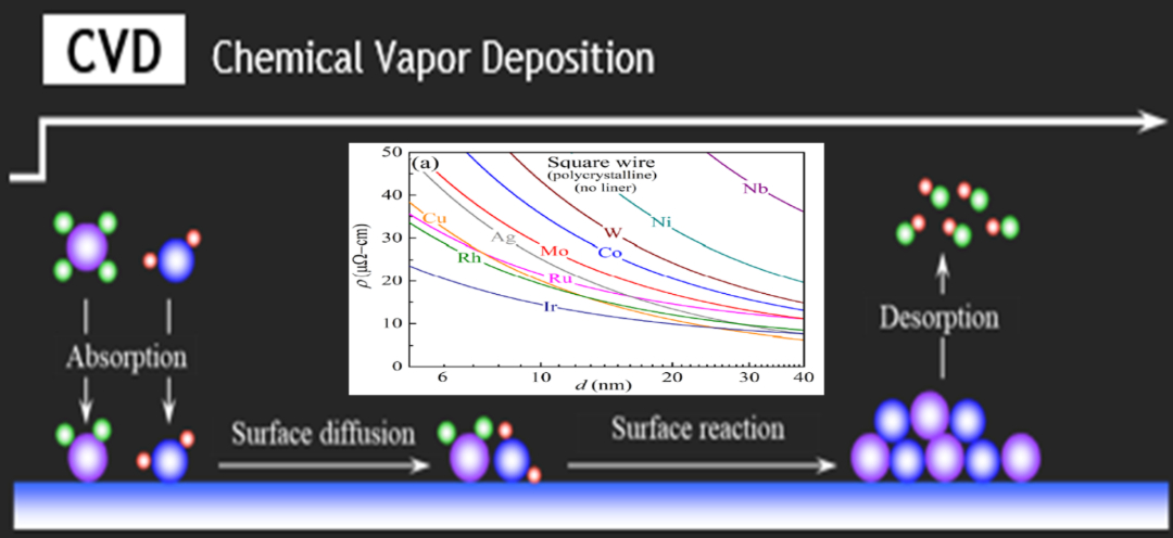
Thinfilm Materials- Next-Generation Metal Development and Improvement of Deposition Uniformity
- Improving thin-film performance efficiency through adhesion control of single-element units based on CVD and sputtering in single-type equipment, and minimizing impurities
- Elaboration of the material adhesion principles by sub-board and the adhesion/release mechanisms according to surface conditions
- Surface modification and adsorption efficiency doubling for the refinement of BDE (Bond Dissociation Energy) control, and improving thin-film quality through precise ligand exchange
- Optimization of impurity control through refinement of precursor design and material ligand design for new metal materials, and enhancement of step coverage and gap fill characteristics
- Development of customizable materials with resistance, D/R, S/C, G/F, and Film density.
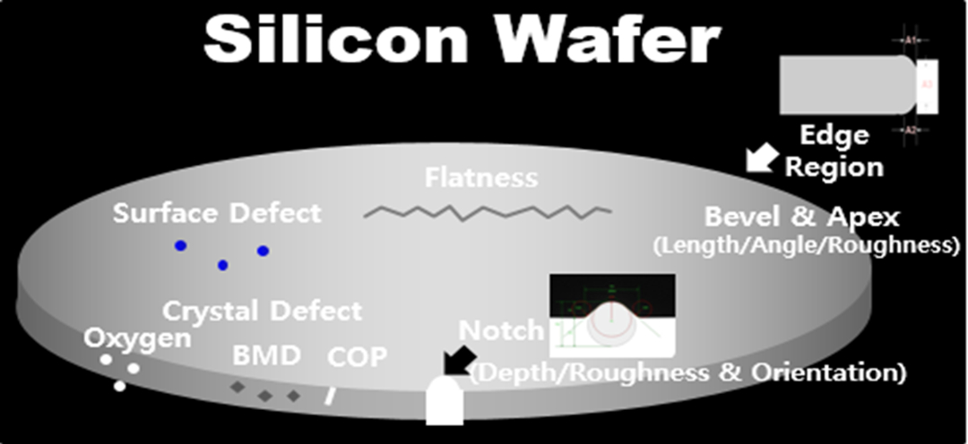
Wafer Materials - Circuit board material that withstands extremes through defect control
- It refers to a single-crystal silicon thin film that serves as the substrate for manufacturing semiconductor chips, and its key quality characteristics include flatness, surface defects, crystal defects, and wafer edge & notch dimensions
- Wafers are classified by size (200 mm, 300 mm), dopant type (N-type, P-type), crystal orientation, and notch position (100, 110, 111), additional processing (polished wafer, epitaxial wafer, SOI wafer), and material (SiC, GaN, SiCOI, GaNOI)
- The wafer manufacturing process is Growing→Cropping & Slicing→Edge Grinding→Lapping & Grinding→Double Side Grinding & Etching → Double Side Polishing & Re-Polishing → Flatness Insp→Final Cleaning →Particle Counting→Epi Growing→Packing
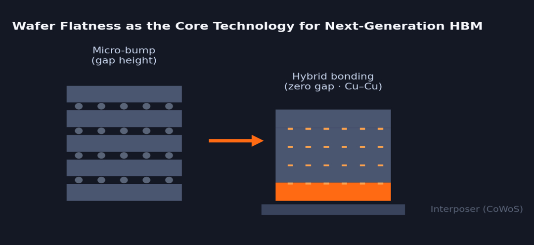
WLP Materials (Wafer Level Package) - Materials package for AI Memory
- Toward next-generation HBM and advanced 2.5D/3D packages, WLP materials serve more process steps under ever-more-severe requirements we optimize front-end materials for package processes and develop WLP-dedicated systems.
- Hybrid-bonding HBM: the shift from gap-height shrink to zero gap makes wafer flatness the core technology.
- Cu CMP slurry optimization and cleaning solutions delivering bond-ready, atomically flat surfaces.
- Next-generation dielectrics for CoWoS-class devices and ultra-high-aspect-ratio patterning materials for advanced integration.
Want to learn more about how we can create new values for semiconductor industry? Please contact us!
We are in this together! Contact Us