'%20fill='%23ea002c'/%3e%3cpath%20d='M31.44,109.48l7.92-9.71H33.72l-6.32,8.38h-.1V99.77H22.65v20.58h.28c2,0,4.4-.93,4.4-4.29v-4.73h.1l6.44,8.76h5.92Z'%20transform='translate(-5.29%20-72.33)'%20fill='%23ea002c'/%3e%3c/g%3e%3cg%3e%3cpath%20d='M39.63,77.72c-1.64.31-4.07,1.8-4.06,4.43,0,2.39,2,3.83,2,7a5.54,5.54,0,0,1-2.69,4.82c.57-.05,1.19-.08,1.87-.08a14.65,14.65,0,0,1,2.35.14l7.35-9A30.51,30.51,0,0,0,39.63,77.72Z'%20transform='translate(-5.29%20-72.33)'%20fill='%23ea002c'/%3e%3cpath%20d='M45.8,102.08c.93-1.44,1-3.74,1.12-6.07s.55-3.83,3.46-3.84c.65,0,1.26.09,2.38.09a17.2,17.2,0,0,0,8.8-2.46A30.54,30.54,0,0,0,46.41,85c-.41,1.18-3.67,10.23-3.92,11a11.32,11.32,0,0,1,1.32,1.93A21.12,21.12,0,0,1,45.8,102.08Z'%20transform='translate(-5.29%20-72.33)'%20fill='%23ea002c'/%3e%3cpath%20d='M30.28,94.69c-.38,0-.56-.25-.61-.68s-1.89-17.24-2.16-19.79c0-.37-.13-1-.13-1.3a.53.53,0,0,1,.55-.59c.87,0,5.62,1.11,10.66,4.64a5.37,5.37,0,0,0-4.07,5c0,2.77,2,4.29,2,7.07C36.54,93.59,31.35,94.69,30.28,94.69Z'%20transform='translate(-5.29%20-72.33)'%20fill='%23ff7a00'/%3e%3cpath%20d='M46.22,103.28a3.7,3.7,0,0,0,.23.51.52.52,0,0,0,.45.28,1.09,1.09,0,0,0,.42-.11l18.06-8.39c.33-.16,1-.45,1.18-.57a.56.56,0,0,0,.31-.49.58.58,0,0,0-.09-.3,18.5,18.5,0,0,0-4.25-3.76,19.07,19.07,0,0,1-9.63,2.78c-1.12,0-1.38-.08-2.14-.07-2.24,0-2.8,1-2.88,2.92,0,.37,0,.87,0,1.42C47.77,99.25,47.56,101.66,46.22,103.28Z'%20transform='translate(-5.29%20-72.33)'%20fill='%23ff7a00'/%3e%3c/g%3e%3cg%3e%3cpath%20d='M70.2,120.63c-1.7,4.61-3.89,5.2-5.78,5.2A5.55,5.55,0,0,1,62,125.3l.71-2.15a3.69,3.69,0,0,0,1.58.42c1.49,0,2.43-.84,3.26-3.44l-5.14-11.21a5.45,5.45,0,0,1,1.39-.21c1.65,0,2,1,2.43,2.06.36.85,2.7,6.51,2.7,6.51H69l2.72-8.36h2.81Z'%20transform='translate(-5.29%20-72.33)'%20fill='%23ff7a00'/%3e%3cpath%20d='M107.43,120.08l-3.93-5.72,3.85-5.6H104l-2.68,4.1-1.61-2.53c-.54-.83-1-1.66-2.25-1.63a2.46,2.46,0,0,0-.52,0,4.83,4.83,0,0,0-1.33.47c0,.06,1.89,2.68,3.65,5.22l-3.88,5.64h3.32l2.7-4.12,2.69,4.12Z'%20transform='translate(-5.29%20-72.33)'%20fill='%23ff7a00'/%3e%3cpath%20d='M76.84,112.6v7.49h2.81V112.3a3.79,3.79,0,0,1,2.26-1.09,2.16,2.16,0,0,1,2.2,2.41v6.47h2.81v-7.17a3.87,3.87,0,0,0-4.08-4.16,5.09,5.09,0,0,0-3.39,1.47A1.81,1.81,0,0,0,77.57,109a5.79,5.79,0,0,0-1,.14A14.85,14.85,0,0,1,76.84,112.6Z'%20transform='translate(-5.29%20-72.33)'%20fill='%23ff7a00'/%3e%3cg%3e%3cpath%20d='M93.2,105.54a1.74,1.74,0,1,1-1.74-1.69A1.71,1.71,0,0,1,93.2,105.54Z'%20transform='translate(-5.29%20-72.33)'%20fill='%23ff7a00'/%3e%3crect%20x='84.78'%20y='36.59'%20width='2.79'%20height='11.16'%20fill='%23ff7a00'/%3e%3c/g%3e%3cpath%20d='M53.44,110.2a5.74,5.74,0,0,1,3.62-1.49c2.19,0,3.8,1.14,3.8,3.91v7.47H57.94v-6.67a2,2,0,0,0-2-2.18,4.24,4.24,0,0,0-2.54,1.21v7.64h-2.9v-17h.62a2.22,2.22,0,0,1,2.28,2.35Z'%20transform='translate(-5.29%20-72.33)'%20fill='%23ff7a00'/%3e%3c/g%3e%3c/g%3e%3c/svg%3e)
Revolutionary Memory
Our core vision is to innovate memory to create a better and sustainable world. Our revolutionary memory research aims to push memory technologies further than ever imagined. Our vision serves as the backbone of SK hynix’s memory roadmap, specifically designed to defy the scaling limits of DRAM and NAND technologies by adopting innovative materials, processes, structures, and products. In addition, new memory technologies, which break the existing frames, will present a new path forward for memory. At SK hynix, we are striding forward with future DRAM, future NAND, and new memory devices to shift the paradigm of memory in the semiconductor industry.
Future DRAM
- FRAM(Ferroelectric RAM) is non-volatile random access memory with DRAM-level speed. World-first 1Xnm half-pitch FE-RAM with 8Gb density was fabricated, and operation was confirmed. We showed that FRAM operation is possible even at low operating voltage using 2Pr from pinched hysteresis of the 5nm- thick ultra-thin HZO capacitor. We confirmed that FRAM cells operate at write time under 80ns and speed characteristics can be improved by Vcore optimization.
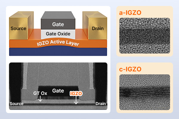
- The InGaZnO channel is attracting attention to improve the refresh characteristics of DRAM. InGaZnO thin film transistors have been used in the display industry for a long time due to their moderate carrier mobility, extremely low leakage current and substrate size scalability. It can be a candidate for a stackable channel material for future DRAM.

SOCAMM2 (Small Outline Compression Attached Memory Module)
Our SOCAMM2 memory solution based on LPDDR, a proven technology to reduce power in mobile application, provides less power consumption and more capacity per module comparing to RDIMM.
Future NAND
- Our research addresses such hurdles by exploring stack height scaling, new materials, and new 3D NAND cell architectures.
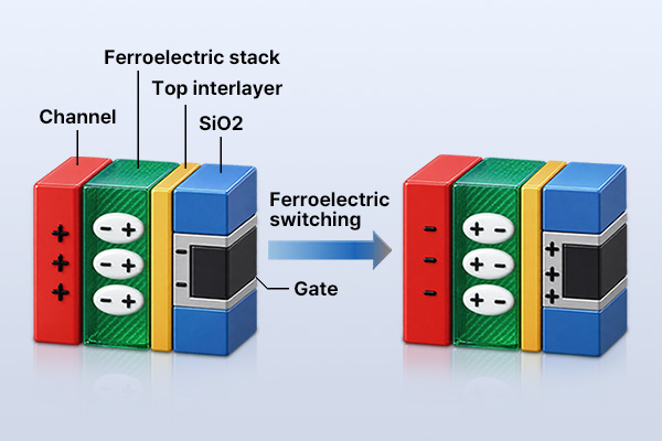
- Examples include applying ferroelectric material to the conventional 3D NAND architecture. We demonstrated the multi-level capable 3D Ferroelectric NAND device using conventional 3D NAND fabrication process, which was published in IMW 2022. Details can be found here. (https://doi.org/10.1109/IMW52921.2022.9779278)
Related Works
![[Summary] Co-Optimizing Cell, Non-Cell, and Page Schemes for Energy Efficient Analog Computing in 3D FeNAND](https://mis-prod-koce-research-user-cdn-01-blob-ep.azureedge.net/web/blog/20251231/thumb_y5dtflR7.20251231154647949.png) Insights
Insights[Summary] Co-Optimizing Cell, Non-Cell, and Page Schemes for Energy Efficient Analog Computing in 3D FeNAND
![[Preview] SK hynix in IEDM 2025](https://mis-prod-koce-research-user-cdn-01-blob-ep.azureedge.net/web/blog/20251124/thumb_t51mgOyH.20251124133523390.png) Insights
Insights[Preview] SK hynix in IEDM 2025
![[Summary] 224 TOPS/W-level Analog Computation in Memory Cell Using Hybrid Ferroelectric Tunnel Junction Having Enhanced On-State Conductance](https://mis-prod-koce-research-user-cdn-01-blob-ep.azureedge.net/web/blog/20250716/thumb_qYH3UUzv.20250716094321913.png) Insights
Insights[Summary] 224 TOPS/W-level Analog Computation in Memory Cell Using Hybrid Ferroelectric Tunnel Junction Having Enhanced On-State Conductance
Want to learn more about how we can create new values for semiconductor industry? Please contact us!
We are in this together! Contact Us