'%20fill='%23ea002c'/%3e%3cpath%20d='M31.44,109.48l7.92-9.71H33.72l-6.32,8.38h-.1V99.77H22.65v20.58h.28c2,0,4.4-.93,4.4-4.29v-4.73h.1l6.44,8.76h5.92Z'%20transform='translate(-5.29%20-72.33)'%20fill='%23ea002c'/%3e%3c/g%3e%3cg%3e%3cpath%20d='M39.63,77.72c-1.64.31-4.07,1.8-4.06,4.43,0,2.39,2,3.83,2,7a5.54,5.54,0,0,1-2.69,4.82c.57-.05,1.19-.08,1.87-.08a14.65,14.65,0,0,1,2.35.14l7.35-9A30.51,30.51,0,0,0,39.63,77.72Z'%20transform='translate(-5.29%20-72.33)'%20fill='%23ea002c'/%3e%3cpath%20d='M45.8,102.08c.93-1.44,1-3.74,1.12-6.07s.55-3.83,3.46-3.84c.65,0,1.26.09,2.38.09a17.2,17.2,0,0,0,8.8-2.46A30.54,30.54,0,0,0,46.41,85c-.41,1.18-3.67,10.23-3.92,11a11.32,11.32,0,0,1,1.32,1.93A21.12,21.12,0,0,1,45.8,102.08Z'%20transform='translate(-5.29%20-72.33)'%20fill='%23ea002c'/%3e%3cpath%20d='M30.28,94.69c-.38,0-.56-.25-.61-.68s-1.89-17.24-2.16-19.79c0-.37-.13-1-.13-1.3a.53.53,0,0,1,.55-.59c.87,0,5.62,1.11,10.66,4.64a5.37,5.37,0,0,0-4.07,5c0,2.77,2,4.29,2,7.07C36.54,93.59,31.35,94.69,30.28,94.69Z'%20transform='translate(-5.29%20-72.33)'%20fill='%23ff7a00'/%3e%3cpath%20d='M46.22,103.28a3.7,3.7,0,0,0,.23.51.52.52,0,0,0,.45.28,1.09,1.09,0,0,0,.42-.11l18.06-8.39c.33-.16,1-.45,1.18-.57a.56.56,0,0,0,.31-.49.58.58,0,0,0-.09-.3,18.5,18.5,0,0,0-4.25-3.76,19.07,19.07,0,0,1-9.63,2.78c-1.12,0-1.38-.08-2.14-.07-2.24,0-2.8,1-2.88,2.92,0,.37,0,.87,0,1.42C47.77,99.25,47.56,101.66,46.22,103.28Z'%20transform='translate(-5.29%20-72.33)'%20fill='%23ff7a00'/%3e%3c/g%3e%3cg%3e%3cpath%20d='M70.2,120.63c-1.7,4.61-3.89,5.2-5.78,5.2A5.55,5.55,0,0,1,62,125.3l.71-2.15a3.69,3.69,0,0,0,1.58.42c1.49,0,2.43-.84,3.26-3.44l-5.14-11.21a5.45,5.45,0,0,1,1.39-.21c1.65,0,2,1,2.43,2.06.36.85,2.7,6.51,2.7,6.51H69l2.72-8.36h2.81Z'%20transform='translate(-5.29%20-72.33)'%20fill='%23ff7a00'/%3e%3cpath%20d='M107.43,120.08l-3.93-5.72,3.85-5.6H104l-2.68,4.1-1.61-2.53c-.54-.83-1-1.66-2.25-1.63a2.46,2.46,0,0,0-.52,0,4.83,4.83,0,0,0-1.33.47c0,.06,1.89,2.68,3.65,5.22l-3.88,5.64h3.32l2.7-4.12,2.69,4.12Z'%20transform='translate(-5.29%20-72.33)'%20fill='%23ff7a00'/%3e%3cpath%20d='M76.84,112.6v7.49h2.81V112.3a3.79,3.79,0,0,1,2.26-1.09,2.16,2.16,0,0,1,2.2,2.41v6.47h2.81v-7.17a3.87,3.87,0,0,0-4.08-4.16,5.09,5.09,0,0,0-3.39,1.47A1.81,1.81,0,0,0,77.57,109a5.79,5.79,0,0,0-1,.14A14.85,14.85,0,0,1,76.84,112.6Z'%20transform='translate(-5.29%20-72.33)'%20fill='%23ff7a00'/%3e%3cg%3e%3cpath%20d='M93.2,105.54a1.74,1.74,0,1,1-1.74-1.69A1.71,1.71,0,0,1,93.2,105.54Z'%20transform='translate(-5.29%20-72.33)'%20fill='%23ff7a00'/%3e%3crect%20x='84.78'%20y='36.59'%20width='2.79'%20height='11.16'%20fill='%23ff7a00'/%3e%3c/g%3e%3cpath%20d='M53.44,110.2a5.74,5.74,0,0,1,3.62-1.49c2.19,0,3.8,1.14,3.8,3.91v7.47H57.94v-6.67a2,2,0,0,0-2-2.18,4.24,4.24,0,0,0-2.54,1.21v7.64h-2.9v-17h.62a2.22,2.22,0,0,1,2.28,2.35Z'%20transform='translate(-5.29%20-72.33)'%20fill='%23ff7a00'/%3e%3c/g%3e%3c/g%3e%3c/svg%3e)


Fusion of Thoughts Leads to Fusion of Technology
Realizing technological innovation suitable for future needs
Blog Spotlight
Current hot topic
See All- Insights[Summary] A Memristor-based In-Memory Computing SoC with Efficient Depthwise Convolution
The rapid growth of AI foundation models has intensified the "memory wall" problem, where constant data movement between processors and memory leads to high power consumption, latency, and heat. To address this, the industry is shifting from "compute-centric" to "memory-centric" architectures. Leading this change, SK hynix (G-RTC) and TetraMem have partnered to implement a next-generation Analog Compute-in-Memory (A-CiM) architecture. This collaboration marks a significant milestone in AI infrastructure by directly tackling data movement inefficiencies. The key achievements of this joint research are summarized in three points:
The first key achievement is the world’s first end-to-end hardware demonstration of Depthwise-Separable Convolution (DSC) on a Resistive Switching Cell (RSC)/CMOS-based System-on-Chip (SoC). By performing matrix operations directly within the memory arrays where AI model weights are stored ("Compute-in-Memory"), this work fundamentally removes the need for data movement and overcomes traditional bottlenecks. While DSC has proven difficult for conventional A-CiM architectures, this design successfully accelerates it on silicon. To enable this, the team proposed a novel Zig-Zag Selection-line (SEL) topology. As detailed in Fig. 1, unlike the straight lines in normal crossbars, the SELs in depthwise arrays are routed in a zig-zag pattern to connect specific transistor gates within the 1T1R cells. This unique wiring allows the architecture to activate cells diagonally, boosting weight utilization in depthwise layers to nearly 100% and facilitating efficient sharing of peripheral circuits. Consequently, signal paths for both depthwise and standard operations are maximized for efficiency across the entire network.
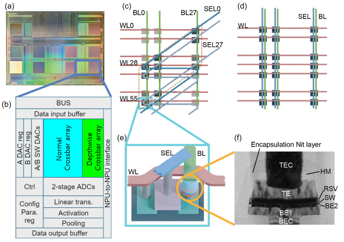
Fig. 1. (a) Optical image of a system-on-chip (SoC). Each chip has 10 NPUs, each containing one 256 × 256 crossbar array. (b) Architecture of one depthwise NPU with eight blocks. Each block includes one 252 × 28 depthwise crossbar. Cells enabled by SEL0 are shown, while other cells are masked with blue. (c) Schematic of one depthwise crossbar. SEL0 is highlighted to show the zig–zag shape of SELs. (d) Schematic of normal 1T1R crossbars. (e) 1T1R cell structure showing the direction of WL, BL, and SEL. (f) Cross-sectional TEM image of the RSC cell fabricated. TEC, TE contact; HM, hard mask; TE, top electrode; RSV, reservoir; SWL, switching layer; BE, bottom electrode; BEC, BE contact.
The second major achievement is the demonstration of exceptional energy efficiency alongside validation on real-world AI models. Fabricated using a standard 65nm CMOS process, the chip delivers 0.254 TOPS per NPU and achieves an energy efficiency of 21.3 TOPS/W at 100MHz (Fig. 2a). This performance delivers more than 10 times the energy efficiency of the NVIDIA A100 GPU, reaching levels comparable to state-of-the-art 28nm SRAM-based CiM accelerators despite the older process node. Furthermore, the chip’s practical viability was confirmed through real-world benchmark testing. When executing the lightweight MobileNetV1 model on the Visual Wake Words (VWW) task, the hardware achieved an inference accuracy of 80.36%. As shown in Fig. 2b, this result is slightly higher than the 4-bit software quantization accuracy (79.34%) and remains stable across repeated runs (80.30%~80.39%), confirming negligible run-to-run variation. This proves that the proposed architecture has advanced beyond a theoretical concept to a fully practical, chip-level platform ready for deployment.
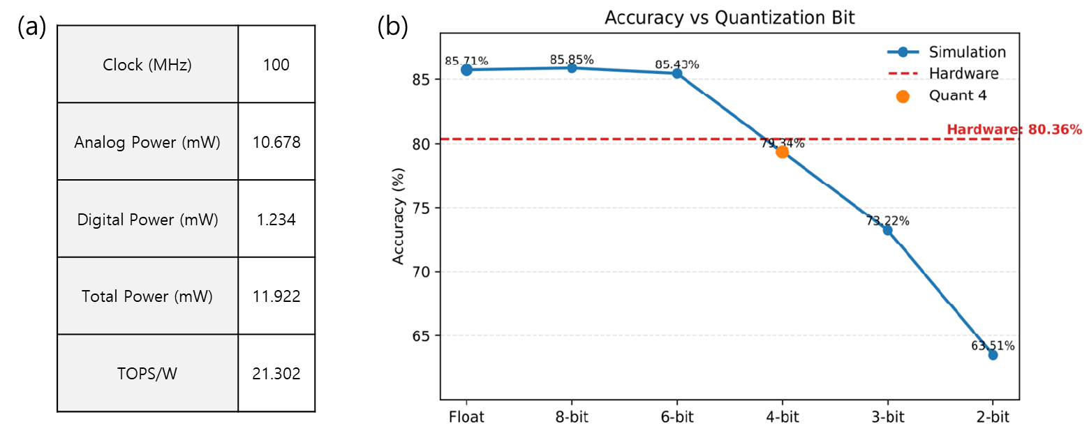
Fig.2. (a) VMM-state power and efficiency summary. (b) Software accuracy as the weight precision is swept from 8 → 2 bits, with the measured hardware point overlaid. The hardware accuracy of 80.36% is slightly higher than the 4-bit quantization accuracy of 79.34%.
The third key achievement is the establishment of a comprehensive "mapping and deployment flow" for complex artificial neural networks. Moving beyond a simple chip demonstration, the team developed an end-to-end software stack that orchestrates layer partitioning, heterogeneous mapping, zig-zag kernel placement, calibration-based programming, and RISC-V-based layer scheduling. As illustrated in Fig. 3, this workflow enables the smooth execution of complex CNN models on the hybrid NPU architecture. The figure details how convolutional layers (e.g., DSConv1~5) are optimally partitioned and distributed across multiple NPU units (labeled NPU0–NPU5), maximizing hardware utilization through efficient kernel placement. This capability marks a significant transition from a prototype to a fully functional platform, proving that intricate AI workloads can be deployed reliably. This achievement stems from close engineering collaboration, merging SK hynix’s deep expertise in memory technology with TetraMem’s advanced A-CiM platform capabilities to deliver a complete AI solution.
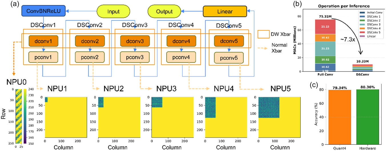
Fig. 3. (a) The MobileNetV1Small architecture and placement of each layer onto the standard or Depthwise NPU. (b) Number of MAC operations per inference for the DSConv model versus an equivalent full-convolution baseline. (c) End-to-end VWW inference accuracy of the fabricated SoC versus the same software model quantized to 4-bit precision.
In conclusion, this research successfully overcame critical hardware design challenges and demonstrated the seamless execution of real-world AI workloads. These achievements were recognized through publication as a Cover Feature in Advanced Intelligent Systems. The developed SoC establishes a solid foundation for sustainable, next-generation memory-centric AI infrastructure, enabling high-efficiency inference from edge devices to future data centers.
The Publication : Link

- Insights[Insights] Evolving Role of Emerging Memories in Next-Generation Computing
- Insights[Summary] Electrical Characteristics of the 4F2 Vertical Gate (VG) DRAM integrated with Bit-Line Shielding (BLS) and Back Gate (BG) Transistor
- Insights[White Paper] Enabling inference at massive scale with hybrid storage for KV cache offloading
NEWS
Open External
Research & Publications
Recent Publications
See All