'%20fill='%23ea002c'/%3e%3cpath%20d='M31.44,109.48l7.92-9.71H33.72l-6.32,8.38h-.1V99.77H22.65v20.58h.28c2,0,4.4-.93,4.4-4.29v-4.73h.1l6.44,8.76h5.92Z'%20transform='translate(-5.29%20-72.33)'%20fill='%23ea002c'/%3e%3c/g%3e%3cg%3e%3cpath%20d='M39.63,77.72c-1.64.31-4.07,1.8-4.06,4.43,0,2.39,2,3.83,2,7a5.54,5.54,0,0,1-2.69,4.82c.57-.05,1.19-.08,1.87-.08a14.65,14.65,0,0,1,2.35.14l7.35-9A30.51,30.51,0,0,0,39.63,77.72Z'%20transform='translate(-5.29%20-72.33)'%20fill='%23ea002c'/%3e%3cpath%20d='M45.8,102.08c.93-1.44,1-3.74,1.12-6.07s.55-3.83,3.46-3.84c.65,0,1.26.09,2.38.09a17.2,17.2,0,0,0,8.8-2.46A30.54,30.54,0,0,0,46.41,85c-.41,1.18-3.67,10.23-3.92,11a11.32,11.32,0,0,1,1.32,1.93A21.12,21.12,0,0,1,45.8,102.08Z'%20transform='translate(-5.29%20-72.33)'%20fill='%23ea002c'/%3e%3cpath%20d='M30.28,94.69c-.38,0-.56-.25-.61-.68s-1.89-17.24-2.16-19.79c0-.37-.13-1-.13-1.3a.53.53,0,0,1,.55-.59c.87,0,5.62,1.11,10.66,4.64a5.37,5.37,0,0,0-4.07,5c0,2.77,2,4.29,2,7.07C36.54,93.59,31.35,94.69,30.28,94.69Z'%20transform='translate(-5.29%20-72.33)'%20fill='%23ff7a00'/%3e%3cpath%20d='M46.22,103.28a3.7,3.7,0,0,0,.23.51.52.52,0,0,0,.45.28,1.09,1.09,0,0,0,.42-.11l18.06-8.39c.33-.16,1-.45,1.18-.57a.56.56,0,0,0,.31-.49.58.58,0,0,0-.09-.3,18.5,18.5,0,0,0-4.25-3.76,19.07,19.07,0,0,1-9.63,2.78c-1.12,0-1.38-.08-2.14-.07-2.24,0-2.8,1-2.88,2.92,0,.37,0,.87,0,1.42C47.77,99.25,47.56,101.66,46.22,103.28Z'%20transform='translate(-5.29%20-72.33)'%20fill='%23ff7a00'/%3e%3c/g%3e%3cg%3e%3cpath%20d='M70.2,120.63c-1.7,4.61-3.89,5.2-5.78,5.2A5.55,5.55,0,0,1,62,125.3l.71-2.15a3.69,3.69,0,0,0,1.58.42c1.49,0,2.43-.84,3.26-3.44l-5.14-11.21a5.45,5.45,0,0,1,1.39-.21c1.65,0,2,1,2.43,2.06.36.85,2.7,6.51,2.7,6.51H69l2.72-8.36h2.81Z'%20transform='translate(-5.29%20-72.33)'%20fill='%23ff7a00'/%3e%3cpath%20d='M107.43,120.08l-3.93-5.72,3.85-5.6H104l-2.68,4.1-1.61-2.53c-.54-.83-1-1.66-2.25-1.63a2.46,2.46,0,0,0-.52,0,4.83,4.83,0,0,0-1.33.47c0,.06,1.89,2.68,3.65,5.22l-3.88,5.64h3.32l2.7-4.12,2.69,4.12Z'%20transform='translate(-5.29%20-72.33)'%20fill='%23ff7a00'/%3e%3cpath%20d='M76.84,112.6v7.49h2.81V112.3a3.79,3.79,0,0,1,2.26-1.09,2.16,2.16,0,0,1,2.2,2.41v6.47h2.81v-7.17a3.87,3.87,0,0,0-4.08-4.16,5.09,5.09,0,0,0-3.39,1.47A1.81,1.81,0,0,0,77.57,109a5.79,5.79,0,0,0-1,.14A14.85,14.85,0,0,1,76.84,112.6Z'%20transform='translate(-5.29%20-72.33)'%20fill='%23ff7a00'/%3e%3cg%3e%3cpath%20d='M93.2,105.54a1.74,1.74,0,1,1-1.74-1.69A1.71,1.71,0,0,1,93.2,105.54Z'%20transform='translate(-5.29%20-72.33)'%20fill='%23ff7a00'/%3e%3crect%20x='84.78'%20y='36.59'%20width='2.79'%20height='11.16'%20fill='%23ff7a00'/%3e%3c/g%3e%3cpath%20d='M53.44,110.2a5.74,5.74,0,0,1,3.62-1.49c2.19,0,3.8,1.14,3.8,3.91v7.47H57.94v-6.67a2,2,0,0,0-2-2.18,4.24,4.24,0,0,0-2.54,1.21v7.64h-2.9v-17h.62a2.22,2.22,0,0,1,2.28,2.35Z'%20transform='translate(-5.29%20-72.33)'%20fill='%23ff7a00'/%3e%3c/g%3e%3c/g%3e%3c/svg%3e)
[Insight] Virtual TEM/SEM Generation Platform for Semiconductor Industry
1. Introduction
If you happen to get an X-ray, a CT scan, or an MRI taken at the hospital, you will notice that your medical expense increases by ten fold in order for higher image resolution. Suppose you paid ten dollars for your X-ray; it will cost you roughly one hundred dollars for a CT scan and one thousand dollars for an MRI scan. You might wonder if there is a way to create a resolution of an MRI that costs as little as a CT scan. There is a deep learning technology that can do just that and is referred to as “Generative Adversarial Network (GAN)” 1)2)3).
Computer vision-related deep learning schemes have found many applications in the semiconductor R&D. In addition, image classification and object detection have been utilized in the semiconductor defect monitoring and detection. Similarly, image segmentation has found a use in semiconductor critical dimension (CD) measurements. Unfortunately, image generation has not found any applications so far when semiconductor R&D heavily relies on the visual inspection of various images such as SEM (Scanning Electron Microscopy) or TEM (Transmission Electron Microscopy). At SK Hynix RTC, we have been interested in virtual visualization using both supervised & unsupervised GAN techniques such as conditional GAN4) and Pix2Pix5).
2. Virtual TEM/SEM Generation Platform
The first example of GAN employment is to simulate semiconductor processing experiments. A significant portion of memory R&D is spent in fine-tuning memory cell profiles. We typically experiment with various etch equipment or hard mask-related source parameters to create the response profile parameters. Usually, many experimentalparameters are being explored with specific domain kowneldge of the processes. domain knowledge Our interest is to generate estimated TEM images of the experiment results before running them in semiconductor processes. As shown in fig.1, two images at both ends are trained and reproduced from the previous actual semiconductor processing experiments. Based on these two points, latent space interpolation was used to generate figures in between. The interpolation coefficient that corresponds to a particular experiment of interest can also be obtained from previous experiments. The major difference between this approach and that of Technology Computer Aided Design (TCAD) is that it doesn't require analytical models. TEM images from previous experiments can enable us to run these types of simulations.
We are excited at the initial feasibility study of image generation based on GAN in semiconductor processes before an actual experiment is done. We would like to continue the research regarding GAN based image generation for the semiconductor processes since this technique may expedite R&D process TAT and help to reach the ESG goals by maximizing ROI.
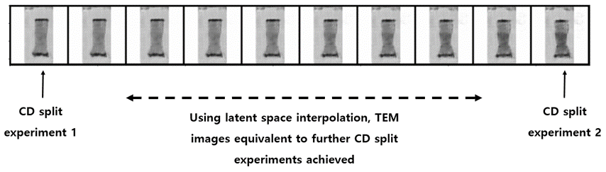
Fig. 1. Two images at both ends are trained and reproduced from the previous actual semiconductor processing experiments Using latent space interpolation of GAN, TEM images equivalent to further CD split experiments achieved
References
1) “Image Synthesis in Multi-Contrast MRI with Conditional Generative Adversarial Networks”, Dar et al., IEEE-TMI (2019)
2) “Learning to Synthesize 7T MRI from 3T MRI with Few Data by Deformable Augmentation”, Wei et al., MLMI (2021)
3) “A Deep Generative-Discriminative Learning for Multimodal Representation in Imaging Genetics”, Ko et al., IEEE-TMI (2022)
4) “Unsupervised Representation Learning with Deep Convolutional Generative Adversarial Networks”, Alec Radford, Luke Metz, Soumith Chintala, arXiv:1511.06434 (2015)
5) "Image-to-Image Translation with Conditional Adversarial Networks”, Phillip Isola, Jun-Yan Zhu, Tinghui Zhou, Alexei A. Efros, arXiv:1611.07004 (2017)
![[Summary] A Memristor-based In-Memory Computing SoC with Efficient Depthwise Convolution](https://mis-prod-koce-research-user-cdn-01-blob-ep.azureedge.net/web/blog/20260806/thumb_sEVmfv3K.20260806085519833.jpg)
![[Insights] Evolving Role of Emerging Memories in Next-Generation Computing](https://mis-prod-koce-research-user-cdn-01-blob-ep.azureedge.net/web/blog/20260806/thumb_NgJoNLYn.20260806080458980.jpg)
![[Summary] Electrical Characteristics of the 4F2 Vertical Gate (VG) DRAM integrated with Bit-Line Shielding (BLS) and Back Gate (BG) Transistor](https://mis-prod-koce-research-user-cdn-01-blob-ep.azureedge.net/web/blog/20260806/thumb_DOUurl5m.20260806080624234.png)