'%20fill='%23ea002c'/%3e%3cpath%20d='M31.44,109.48l7.92-9.71H33.72l-6.32,8.38h-.1V99.77H22.65v20.58h.28c2,0,4.4-.93,4.4-4.29v-4.73h.1l6.44,8.76h5.92Z'%20transform='translate(-5.29%20-72.33)'%20fill='%23ea002c'/%3e%3c/g%3e%3cg%3e%3cpath%20d='M39.63,77.72c-1.64.31-4.07,1.8-4.06,4.43,0,2.39,2,3.83,2,7a5.54,5.54,0,0,1-2.69,4.82c.57-.05,1.19-.08,1.87-.08a14.65,14.65,0,0,1,2.35.14l7.35-9A30.51,30.51,0,0,0,39.63,77.72Z'%20transform='translate(-5.29%20-72.33)'%20fill='%23ea002c'/%3e%3cpath%20d='M45.8,102.08c.93-1.44,1-3.74,1.12-6.07s.55-3.83,3.46-3.84c.65,0,1.26.09,2.38.09a17.2,17.2,0,0,0,8.8-2.46A30.54,30.54,0,0,0,46.41,85c-.41,1.18-3.67,10.23-3.92,11a11.32,11.32,0,0,1,1.32,1.93A21.12,21.12,0,0,1,45.8,102.08Z'%20transform='translate(-5.29%20-72.33)'%20fill='%23ea002c'/%3e%3cpath%20d='M30.28,94.69c-.38,0-.56-.25-.61-.68s-1.89-17.24-2.16-19.79c0-.37-.13-1-.13-1.3a.53.53,0,0,1,.55-.59c.87,0,5.62,1.11,10.66,4.64a5.37,5.37,0,0,0-4.07,5c0,2.77,2,4.29,2,7.07C36.54,93.59,31.35,94.69,30.28,94.69Z'%20transform='translate(-5.29%20-72.33)'%20fill='%23ff7a00'/%3e%3cpath%20d='M46.22,103.28a3.7,3.7,0,0,0,.23.51.52.52,0,0,0,.45.28,1.09,1.09,0,0,0,.42-.11l18.06-8.39c.33-.16,1-.45,1.18-.57a.56.56,0,0,0,.31-.49.58.58,0,0,0-.09-.3,18.5,18.5,0,0,0-4.25-3.76,19.07,19.07,0,0,1-9.63,2.78c-1.12,0-1.38-.08-2.14-.07-2.24,0-2.8,1-2.88,2.92,0,.37,0,.87,0,1.42C47.77,99.25,47.56,101.66,46.22,103.28Z'%20transform='translate(-5.29%20-72.33)'%20fill='%23ff7a00'/%3e%3c/g%3e%3cg%3e%3cpath%20d='M70.2,120.63c-1.7,4.61-3.89,5.2-5.78,5.2A5.55,5.55,0,0,1,62,125.3l.71-2.15a3.69,3.69,0,0,0,1.58.42c1.49,0,2.43-.84,3.26-3.44l-5.14-11.21a5.45,5.45,0,0,1,1.39-.21c1.65,0,2,1,2.43,2.06.36.85,2.7,6.51,2.7,6.51H69l2.72-8.36h2.81Z'%20transform='translate(-5.29%20-72.33)'%20fill='%23ff7a00'/%3e%3cpath%20d='M107.43,120.08l-3.93-5.72,3.85-5.6H104l-2.68,4.1-1.61-2.53c-.54-.83-1-1.66-2.25-1.63a2.46,2.46,0,0,0-.52,0,4.83,4.83,0,0,0-1.33.47c0,.06,1.89,2.68,3.65,5.22l-3.88,5.64h3.32l2.7-4.12,2.69,4.12Z'%20transform='translate(-5.29%20-72.33)'%20fill='%23ff7a00'/%3e%3cpath%20d='M76.84,112.6v7.49h2.81V112.3a3.79,3.79,0,0,1,2.26-1.09,2.16,2.16,0,0,1,2.2,2.41v6.47h2.81v-7.17a3.87,3.87,0,0,0-4.08-4.16,5.09,5.09,0,0,0-3.39,1.47A1.81,1.81,0,0,0,77.57,109a5.79,5.79,0,0,0-1,.14A14.85,14.85,0,0,1,76.84,112.6Z'%20transform='translate(-5.29%20-72.33)'%20fill='%23ff7a00'/%3e%3cg%3e%3cpath%20d='M93.2,105.54a1.74,1.74,0,1,1-1.74-1.69A1.71,1.71,0,0,1,93.2,105.54Z'%20transform='translate(-5.29%20-72.33)'%20fill='%23ff7a00'/%3e%3crect%20x='84.78'%20y='36.59'%20width='2.79'%20height='11.16'%20fill='%23ff7a00'/%3e%3c/g%3e%3cpath%20d='M53.44,110.2a5.74,5.74,0,0,1,3.62-1.49c2.19,0,3.8,1.14,3.8,3.91v7.47H57.94v-6.67a2,2,0,0,0-2-2.18,4.24,4.24,0,0,0-2.54,1.21v7.64h-2.9v-17h.62a2.22,2.22,0,0,1,2.28,2.35Z'%20transform='translate(-5.29%20-72.33)'%20fill='%23ff7a00'/%3e%3c/g%3e%3c/g%3e%3c/svg%3e)
[Summary] Electrical Characteristics of the 4F2 Vertical Gate (VG) DRAM integrated with Bit-Line Shielding (BLS) and Back Gate (BG) Transistor
DRAM has been evolving in cell architecture to improve its density, speed, and power characteristics. Conventional DRAM cell transistor based on buried-gate structure faces fundamental scaling limits due to increased process complexity and degradation of device performance in the range of sub-10nm technology nodes. To overcome these challenges, 4F2 VG DRAM has emerged as a promising solution to extend DRAM scaling beyond current scaling limits. In this report, electrical characteristics of 4F2 VG DRAM are reviewed with key integration features such as bit-line shielding (BLS) and back-gate (BG) structures.
Fig. 1 shows illustrated concept and fabricated 4F2 DRAM structure with peri-under-cell (PUC) architecture where VG cell transistor and peripheral devices are connected through fusion wafer bonding and inter-wafer contact process techniques. This integration scheme enables accurate electrical characterization of VG cell transistor as well as functional verification of product-level operation.
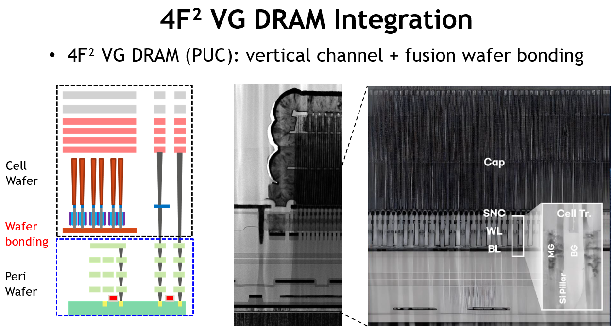
Fig. 1 Structure of 4F2 DRAM with peri-under-cell (PUC) architecture
Back gate (BG) integrated in VG cell transistors enables Vth modulation and suppresses electric field interference induced by biasing of adjacent word-lines (WLs). Fig. 2 shows structures of VG cell transistor with and without BG implementation. As shown in TEM images, BG is positioned between two WL pillars and is shared between the neighboring cells without increasing unit cell size.
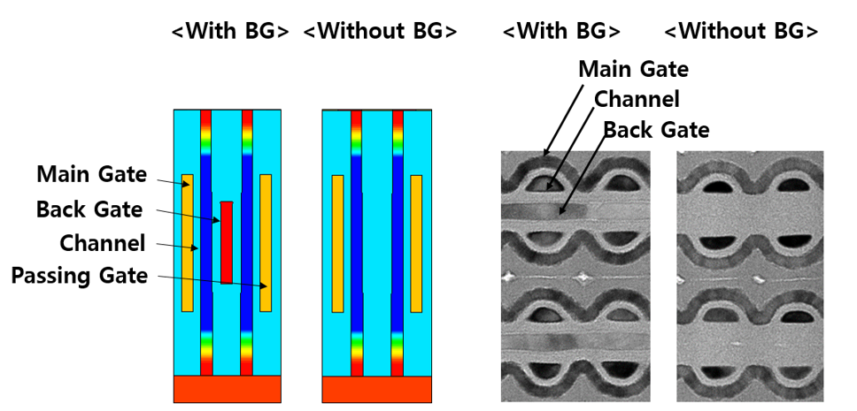
Fig. 2 Structure of Shared Back Gate (BG)
As shown in Fig. 3, shared BG improved threshold voltage modulation by applying a back-bias and it suppresses the electric field coupling from adjacent word line biasing, improving electrostatic integrity of the cell transistor. BG also introduces trade-offs of cell transistor performance such as degradation of on-current and sub-threshold swing.
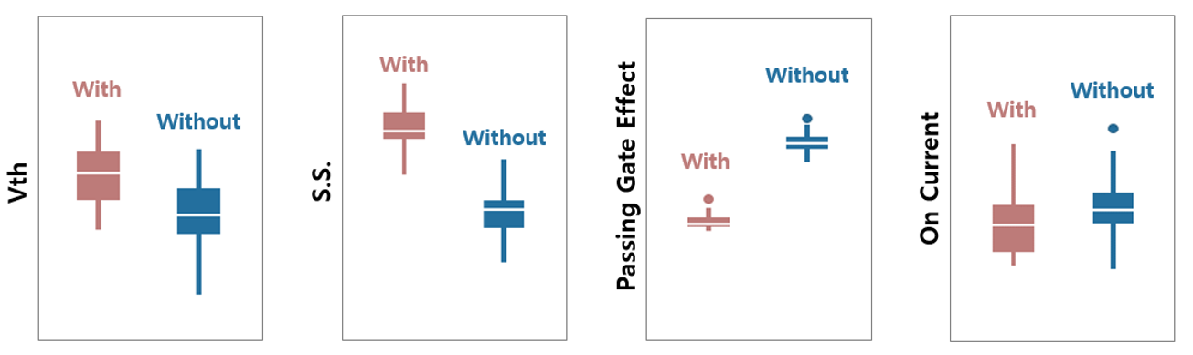
Fig. 3 Back Gate (BG) Effect on Cell Functionality
In VG cell architecture, parasitic capacitance in between bit-lines increases drastically as a consequence of the compact VG layout where BLs are routed vertically in close proximity. To address this issue, structural solution for elevated sensing noise was proposed. Fig 4 shows conceptual design of bit-line shielding (BLS) circuit and TEM images of BLS structure employed in this work.
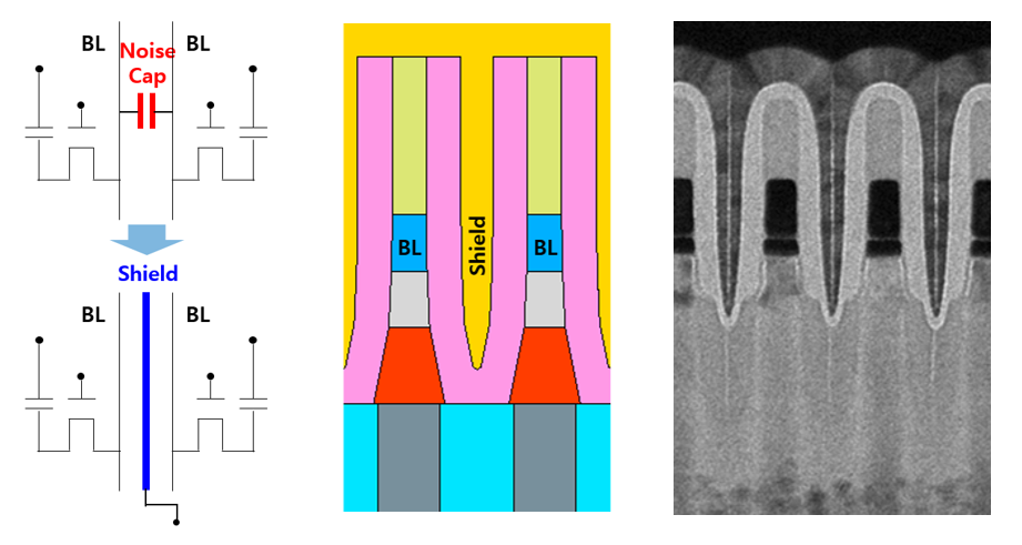
Fig. 4 Bit-line Shielding (BLS) Structure
BLS structure implemented between adjacent BLs substantially reduces effective BL-to-BL coupling noise, resulting in enhancement of sensing capability and significant reduction in sensing failures, as demonstrated in Fig. 5.
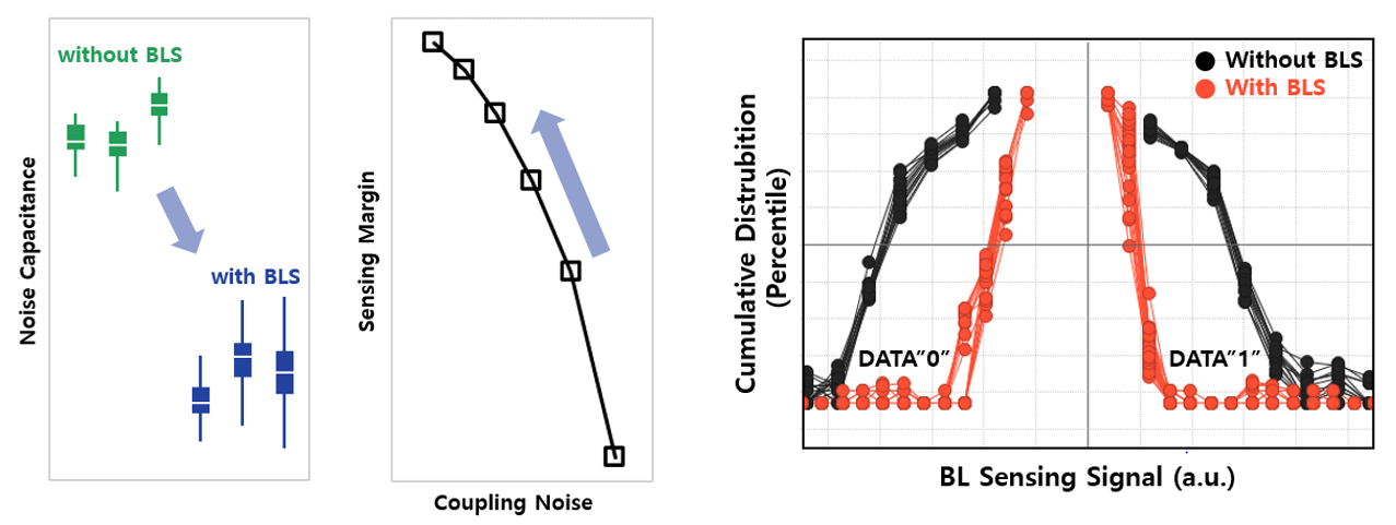
Fig. 5 Sensing Performance of 4F2 VG DRAM with BLS
In summary, 4F2 VG DRAM array in PUC architecture is successfully demonstrated as a promising candidate for future high-density memory applications. Robust performance of cell transistor and read-write operation of 4F2 VG DRAM is successfully achieved. Effect of shared BG in between adjacent two WLs was systematically evaluated to optimize device characteristics and cell functionality. In addition, feasibility and performance benefits of BLS was verified with effective suppression of inter-BL coupling noise.

![[Summary] A Memristor-based In-Memory Computing SoC with Efficient Depthwise Convolution](https://mis-prod-koce-research-user-cdn-01-blob-ep.azureedge.net/web/blog/20260806/thumb_sEVmfv3K.20260806085519833.jpg)
![[Insights] Evolving Role of Emerging Memories in Next-Generation Computing](https://mis-prod-koce-research-user-cdn-01-blob-ep.azureedge.net/web/blog/20260806/thumb_NgJoNLYn.20260806080458980.jpg)
![[White Paper] Enabling inference at massive scale with hybrid storage for KV cache offloading](https://mis-prod-koce-research-user-cdn-01-blob-ep.azureedge.net/web/blog/20260701/thumb_t3l2usp3.20260701105145200.jpg)