'%20fill='%23ea002c'/%3e%3cpath%20d='M31.44,109.48l7.92-9.71H33.72l-6.32,8.38h-.1V99.77H22.65v20.58h.28c2,0,4.4-.93,4.4-4.29v-4.73h.1l6.44,8.76h5.92Z'%20transform='translate(-5.29%20-72.33)'%20fill='%23ea002c'/%3e%3c/g%3e%3cg%3e%3cpath%20d='M39.63,77.72c-1.64.31-4.07,1.8-4.06,4.43,0,2.39,2,3.83,2,7a5.54,5.54,0,0,1-2.69,4.82c.57-.05,1.19-.08,1.87-.08a14.65,14.65,0,0,1,2.35.14l7.35-9A30.51,30.51,0,0,0,39.63,77.72Z'%20transform='translate(-5.29%20-72.33)'%20fill='%23ea002c'/%3e%3cpath%20d='M45.8,102.08c.93-1.44,1-3.74,1.12-6.07s.55-3.83,3.46-3.84c.65,0,1.26.09,2.38.09a17.2,17.2,0,0,0,8.8-2.46A30.54,30.54,0,0,0,46.41,85c-.41,1.18-3.67,10.23-3.92,11a11.32,11.32,0,0,1,1.32,1.93A21.12,21.12,0,0,1,45.8,102.08Z'%20transform='translate(-5.29%20-72.33)'%20fill='%23ea002c'/%3e%3cpath%20d='M30.28,94.69c-.38,0-.56-.25-.61-.68s-1.89-17.24-2.16-19.79c0-.37-.13-1-.13-1.3a.53.53,0,0,1,.55-.59c.87,0,5.62,1.11,10.66,4.64a5.37,5.37,0,0,0-4.07,5c0,2.77,2,4.29,2,7.07C36.54,93.59,31.35,94.69,30.28,94.69Z'%20transform='translate(-5.29%20-72.33)'%20fill='%23ff7a00'/%3e%3cpath%20d='M46.22,103.28a3.7,3.7,0,0,0,.23.51.52.52,0,0,0,.45.28,1.09,1.09,0,0,0,.42-.11l18.06-8.39c.33-.16,1-.45,1.18-.57a.56.56,0,0,0,.31-.49.58.58,0,0,0-.09-.3,18.5,18.5,0,0,0-4.25-3.76,19.07,19.07,0,0,1-9.63,2.78c-1.12,0-1.38-.08-2.14-.07-2.24,0-2.8,1-2.88,2.92,0,.37,0,.87,0,1.42C47.77,99.25,47.56,101.66,46.22,103.28Z'%20transform='translate(-5.29%20-72.33)'%20fill='%23ff7a00'/%3e%3c/g%3e%3cg%3e%3cpath%20d='M70.2,120.63c-1.7,4.61-3.89,5.2-5.78,5.2A5.55,5.55,0,0,1,62,125.3l.71-2.15a3.69,3.69,0,0,0,1.58.42c1.49,0,2.43-.84,3.26-3.44l-5.14-11.21a5.45,5.45,0,0,1,1.39-.21c1.65,0,2,1,2.43,2.06.36.85,2.7,6.51,2.7,6.51H69l2.72-8.36h2.81Z'%20transform='translate(-5.29%20-72.33)'%20fill='%23ff7a00'/%3e%3cpath%20d='M107.43,120.08l-3.93-5.72,3.85-5.6H104l-2.68,4.1-1.61-2.53c-.54-.83-1-1.66-2.25-1.63a2.46,2.46,0,0,0-.52,0,4.83,4.83,0,0,0-1.33.47c0,.06,1.89,2.68,3.65,5.22l-3.88,5.64h3.32l2.7-4.12,2.69,4.12Z'%20transform='translate(-5.29%20-72.33)'%20fill='%23ff7a00'/%3e%3cpath%20d='M76.84,112.6v7.49h2.81V112.3a3.79,3.79,0,0,1,2.26-1.09,2.16,2.16,0,0,1,2.2,2.41v6.47h2.81v-7.17a3.87,3.87,0,0,0-4.08-4.16,5.09,5.09,0,0,0-3.39,1.47A1.81,1.81,0,0,0,77.57,109a5.79,5.79,0,0,0-1,.14A14.85,14.85,0,0,1,76.84,112.6Z'%20transform='translate(-5.29%20-72.33)'%20fill='%23ff7a00'/%3e%3cg%3e%3cpath%20d='M93.2,105.54a1.74,1.74,0,1,1-1.74-1.69A1.71,1.71,0,0,1,93.2,105.54Z'%20transform='translate(-5.29%20-72.33)'%20fill='%23ff7a00'/%3e%3crect%20x='84.78'%20y='36.59'%20width='2.79'%20height='11.16'%20fill='%23ff7a00'/%3e%3c/g%3e%3cpath%20d='M53.44,110.2a5.74,5.74,0,0,1,3.62-1.49c2.19,0,3.8,1.14,3.8,3.91v7.47H57.94v-6.67a2,2,0,0,0-2-2.18,4.24,4.24,0,0,0-2.54,1.21v7.64h-2.9v-17h.62a2.22,2.22,0,0,1,2.28,2.35Z'%20transform='translate(-5.29%20-72.33)'%20fill='%23ff7a00'/%3e%3c/g%3e%3c/g%3e%3c/svg%3e)
[Summary] A Highly Scalable Isolated Charge Trap Nitride Layer Implemented in a 176-layer 3D NAND Flash with Superior Threshold Voltage Distribution and Charge Retention
This article is based on the paper “A Highly Scalable Isolated Charge Trap Nitride Layer Implemented in a 176-layer 3D NAND Flash with Superior Threshold Voltage Distribution and Charge Retention” by Sangwan Jin et al., presented at IEDM 2025. The purpose of this article is to introduce and highlight the technological achievements of SK hynix for industry-wide awareness and contribution.
The aggressive scaling of stack height to enhance 3D NAND density has led to severe issues like high-aspect-ratio etching and wafer warpage. To overcome these challenges, the industry has adopted a strategy of reducing the tier pitch. However, this reduction has intensified cell-to-cell interference and degraded reliability, indicating that tier pitch scaling is now reaching its fundamental limit. To combat the increased cell-to-cell interference caused by aggressive tier pitch scaling, this work employs a Charge Trap Nitride Isolation (CTI) technique. While prior research has demonstrated CTI's effectiveness in low-stack test vehicles, practical solutions for high-layer 3D NAND have been absent. This work bridges that gap by presenting a novel CTI architecture, implemented and evaluated on a 176-layer test vehicle—the highest stack count reported in such studies.
The conventional CTI scheme formed a pocket to isolate the Charge Trap Nitride (CTN) by recessing the mold nitride. However, this approach had critical drawbacks for commercialization, including channel hole enlargement and significant process variation. In contrast, our novel technique forms the pocket on the inner side of the plug through a series of deposition processes, effectively preventing any increase in the channel hole size (Fig. 1). While direct comparative metrology data is limited, process experience and electrical results from 176-layer devices indicate this method achieves superior pocket uniformity.
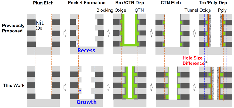
Fig 1. Schematic illustration of the CTI process flow, comparing the previously proposed scheme with the approach developed in this work.
To validate our CTI scheme, we compared our optimized CTI cells with conventional CTN cells across various CTN thicknesses. After TLC programming, CTI cells show a narrower threshold voltage (Vth) distribution and lower sensitivity to CTN thickness — thanks to 30% reduced Cell to Cell (CtC) interference. Across multiple wafers, CTI cells improve within-wafer Vth uniformity by 6.9% while matching conventional CTN Cell’s top-to-bottom consistency. At every program verify level and across all word lines, CTI cells consistently deliver tighter Vth distributions without compromising uniformity (Fig. 2).
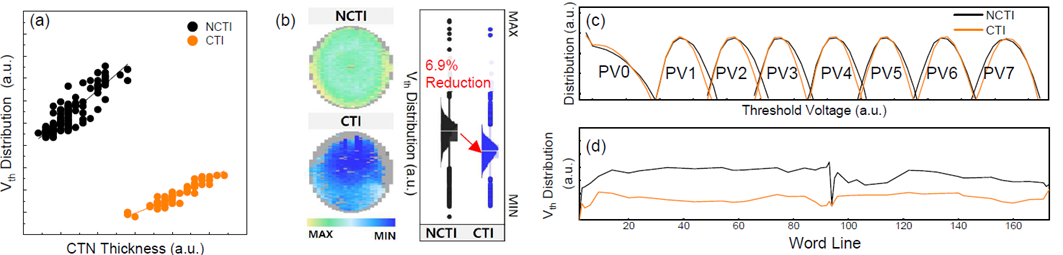
Fig 2. (a) The experimental Vth distribution after TLC programming according to CTN thickness. (b) The within-wafer Vth distribution map and its box plot from CTI and NCTI wafers. (c) The typical Vth distribution of CTI and NCTI cells after TLC programming. (d) The Vth distribution according to WLs. (NCTI denotes conventional non-CTI cells)
Beyond reducing interference, the CTI structure enhances retention by replacing continuous CTN with spacer oxide — minimizing spacer holes that trigger electron spreading and blocking lateral charge paths between cells. TCAD simulations show that while CTN separation slightly increases vertical charge loss, the dramatic drop in lateral loss results in net retention improvement. Experimentally, after 12-hour baking at 125°C, CTI cells show 40% less Vth shift across all CTN thicknesses, with reduced thickness sensitivity confirming CTI’s effectiveness in suppressing lateral charge spread (Fig. 3).
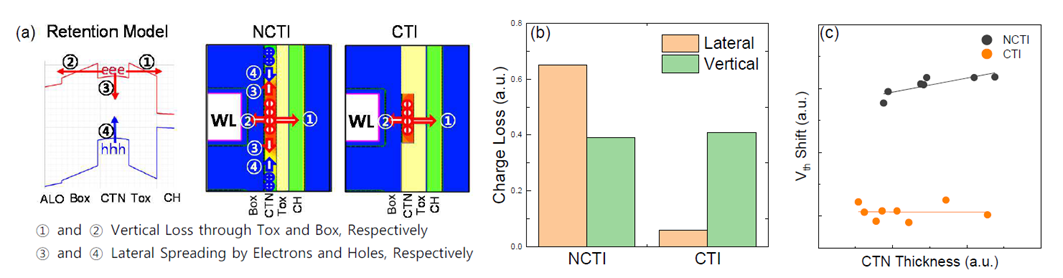
Fig 3. (a) Charge retention mechanism of CTI and NCTI cells. (b) The TCAD prediction of charge loss of NCTI and CTI cells. (c) Vth shift from 125 °C, 12-hour baking retention of NCTI and CTI cells with respect to CTN thickness.
Using TCAD simulations, we projected how CtC interference, Vth distribution, and retention evolve under aggressive tier pitch scaling beyond NCTI’s limits. As tier pitch shrinks, NCTI cells show sharp rises in interference and Vth spread — while CTI drastically lowers both the absolute values and their sensitivity to scaling. This suggests a 4 nm tighter pitch is viable without degrading Vth uniformity. For retention, CTI enables scaling beyond 10 nm reduction, as shown in Fig. 4.
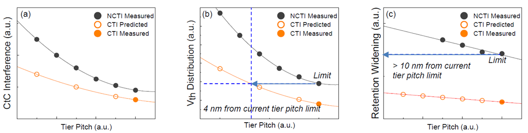
Fig 4. (a) CtC interference, (b) Vth distribution, (c) Retention widening as a function of tier pitch.
In summary, we successfully implemented a highly scalable novel CTI structure in a 176-layer 3D NAND. Reduced CtC interference improved Vth distribution, enabling tighter tier pitches without degradation. Enhanced retention further supports scaling beyond current limits. High yield and uniform Vth across wafers confirm CTI’s manufacturability and scalability — making it a viable solution for next-generation 3D NAND scaling.
The Publication : Link

![[Summary] A Memristor-based In-Memory Computing SoC with Efficient Depthwise Convolution](https://mis-prod-koce-research-user-cdn-01-blob-ep.azureedge.net/web/blog/20260806/thumb_sEVmfv3K.20260806085519833.jpg)
![[Insights] Evolving Role of Emerging Memories in Next-Generation Computing](https://mis-prod-koce-research-user-cdn-01-blob-ep.azureedge.net/web/blog/20260806/thumb_NgJoNLYn.20260806080458980.jpg)
![[Summary] Electrical Characteristics of the 4F2 Vertical Gate (VG) DRAM integrated with Bit-Line Shielding (BLS) and Back Gate (BG) Transistor](https://mis-prod-koce-research-user-cdn-01-blob-ep.azureedge.net/web/blog/20260806/thumb_DOUurl5m.20260806080624234.png)