'%20fill='%23ea002c'/%3e%3cpath%20d='M31.44,109.48l7.92-9.71H33.72l-6.32,8.38h-.1V99.77H22.65v20.58h.28c2,0,4.4-.93,4.4-4.29v-4.73h.1l6.44,8.76h5.92Z'%20transform='translate(-5.29%20-72.33)'%20fill='%23ea002c'/%3e%3c/g%3e%3cg%3e%3cpath%20d='M39.63,77.72c-1.64.31-4.07,1.8-4.06,4.43,0,2.39,2,3.83,2,7a5.54,5.54,0,0,1-2.69,4.82c.57-.05,1.19-.08,1.87-.08a14.65,14.65,0,0,1,2.35.14l7.35-9A30.51,30.51,0,0,0,39.63,77.72Z'%20transform='translate(-5.29%20-72.33)'%20fill='%23ea002c'/%3e%3cpath%20d='M45.8,102.08c.93-1.44,1-3.74,1.12-6.07s.55-3.83,3.46-3.84c.65,0,1.26.09,2.38.09a17.2,17.2,0,0,0,8.8-2.46A30.54,30.54,0,0,0,46.41,85c-.41,1.18-3.67,10.23-3.92,11a11.32,11.32,0,0,1,1.32,1.93A21.12,21.12,0,0,1,45.8,102.08Z'%20transform='translate(-5.29%20-72.33)'%20fill='%23ea002c'/%3e%3cpath%20d='M30.28,94.69c-.38,0-.56-.25-.61-.68s-1.89-17.24-2.16-19.79c0-.37-.13-1-.13-1.3a.53.53,0,0,1,.55-.59c.87,0,5.62,1.11,10.66,4.64a5.37,5.37,0,0,0-4.07,5c0,2.77,2,4.29,2,7.07C36.54,93.59,31.35,94.69,30.28,94.69Z'%20transform='translate(-5.29%20-72.33)'%20fill='%23ff7a00'/%3e%3cpath%20d='M46.22,103.28a3.7,3.7,0,0,0,.23.51.52.52,0,0,0,.45.28,1.09,1.09,0,0,0,.42-.11l18.06-8.39c.33-.16,1-.45,1.18-.57a.56.56,0,0,0,.31-.49.58.58,0,0,0-.09-.3,18.5,18.5,0,0,0-4.25-3.76,19.07,19.07,0,0,1-9.63,2.78c-1.12,0-1.38-.08-2.14-.07-2.24,0-2.8,1-2.88,2.92,0,.37,0,.87,0,1.42C47.77,99.25,47.56,101.66,46.22,103.28Z'%20transform='translate(-5.29%20-72.33)'%20fill='%23ff7a00'/%3e%3c/g%3e%3cg%3e%3cpath%20d='M70.2,120.63c-1.7,4.61-3.89,5.2-5.78,5.2A5.55,5.55,0,0,1,62,125.3l.71-2.15a3.69,3.69,0,0,0,1.58.42c1.49,0,2.43-.84,3.26-3.44l-5.14-11.21a5.45,5.45,0,0,1,1.39-.21c1.65,0,2,1,2.43,2.06.36.85,2.7,6.51,2.7,6.51H69l2.72-8.36h2.81Z'%20transform='translate(-5.29%20-72.33)'%20fill='%23ff7a00'/%3e%3cpath%20d='M107.43,120.08l-3.93-5.72,3.85-5.6H104l-2.68,4.1-1.61-2.53c-.54-.83-1-1.66-2.25-1.63a2.46,2.46,0,0,0-.52,0,4.83,4.83,0,0,0-1.33.47c0,.06,1.89,2.68,3.65,5.22l-3.88,5.64h3.32l2.7-4.12,2.69,4.12Z'%20transform='translate(-5.29%20-72.33)'%20fill='%23ff7a00'/%3e%3cpath%20d='M76.84,112.6v7.49h2.81V112.3a3.79,3.79,0,0,1,2.26-1.09,2.16,2.16,0,0,1,2.2,2.41v6.47h2.81v-7.17a3.87,3.87,0,0,0-4.08-4.16,5.09,5.09,0,0,0-3.39,1.47A1.81,1.81,0,0,0,77.57,109a5.79,5.79,0,0,0-1,.14A14.85,14.85,0,0,1,76.84,112.6Z'%20transform='translate(-5.29%20-72.33)'%20fill='%23ff7a00'/%3e%3cg%3e%3cpath%20d='M93.2,105.54a1.74,1.74,0,1,1-1.74-1.69A1.71,1.71,0,0,1,93.2,105.54Z'%20transform='translate(-5.29%20-72.33)'%20fill='%23ff7a00'/%3e%3crect%20x='84.78'%20y='36.59'%20width='2.79'%20height='11.16'%20fill='%23ff7a00'/%3e%3c/g%3e%3cpath%20d='M53.44,110.2a5.74,5.74,0,0,1,3.62-1.49c2.19,0,3.8,1.14,3.8,3.91v7.47H57.94v-6.67a2,2,0,0,0-2-2.18,4.24,4.24,0,0,0-2.54,1.21v7.64h-2.9v-17h.62a2.22,2.22,0,0,1,2.28,2.35Z'%20transform='translate(-5.29%20-72.33)'%20fill='%23ff7a00'/%3e%3c/g%3e%3c/g%3e%3c/svg%3e)
[Summary] Analog Computation in Ultra-High Density 3D FeNAND for TB-level Hyperscale AI Models
Large language models have become prominent in generating and comprehending human-like text. Their model sizes have been dramatically increasing, even reaching trillions of parameters. The exponential growth in model size needs to have substantial memory resources to handle the vast amounts of data involved in AI inference process. In this regard, 3D vertical NAND string structures (Fig. 1 (a)), known for its high areal density and non-volatile, emerge as a potential candidate for energy efficient analog compute-in-memory (ACiM). These vertical NAND structures especially provide a density advantage by utilizing the same peripheral circuits with digital, ADC, and MUX even as the number of cell layers increases, avoiding additional area requirement (Fig. 1 (b)).
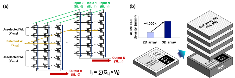
Fig. 1. (a) Schematic illustration of 3D FeNAND array for ACiM, (c) Comparison of cell density of 2D array vs 3D array
In this work, we demonstrated an analog computation in high-density 3D vertical ferroelectric NAND (FeNAND) for the first time. In the vertical string structure of 3D NAND arrays, as the number of word line (WL) stacks increases, the available conductance ranges for analog states decrease (Fig. 2 (a)). Higher subthreshold slope (SS) of FeNAND cells can induce more conductance states with lower input variation then low SS, improving the analog properties of FeNAND cells. In order to make more conductance states, the interface state density within the FeNAND gate stacks was engineered (Fig. 2 (b)). As a results, the SS of 3D FeNAND S2 was up to twice as large as S1 at maximum (Fig. 2 (c)).
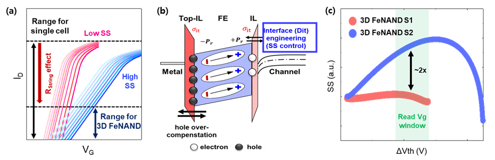
Fig. 2. (a) Schematic illustration of 3D FeNAND string and available current range for multi-leveling. (b) Gate stack of 3D FeNAND with interface engineering. (c) Subthreshold slope as a function of ∆Vth on Split 1 and 2.
The ID-VG curves were measured as a function of program bias amplitude with fixed pulse width for both S1 and S2 of 3D FeNAND (Fig. 3 (a)). The conductance states of 3D FeNAND S1 and 3D FeNAND S2 were confirmed to have ≥128 and ≥256 levels/cell, respectively (Fig. 3 (b)). Furthermore, we verified MAC operations of 3D FeNAND arrays by using Ohm’s law and Kirchhoff's law (MAC currents [IMAC] = Σ[G×V]) (Fig. 3 (c)). The 3D FeNAND arrays with R1 exhibited higher MAC accuracy (87.8 ± 8.2%) than those with R2 (78.4 ± 6.1%) because the R1 conditions are more resilient to IR drop effects than the R2 conditions.
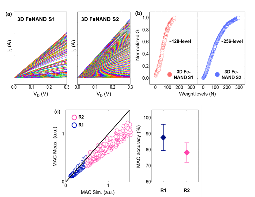
Fig. 3. (a) Measured ID-VD curves with various PGM bias and (b) Conductance as a function of pulse numbers in 3D FeNAND S1 and S2. (c) Experimental data of MAC operations and MAC accuracy in 3D FeNAND.
The simulation revealed that the inference accuracy of all samples (85.7% for 3D FeNAND S1, 85.6% for 3D FeNAND S2, and 85.4% for 2D ReRAM) was similar to the software level inference accuracy (90.3% for FP32 and 89.4% for 4-bit integer post-training-quantization) (Fig. 4 (a)). With the assumption that the weight parameters were all written in cell arrays to reduce data movements, 2D arrays require over 4,000 times more area than 3D arrays for inference (Fig. 4 (b)). The 3D FeNAND arrays exhibited 1000-fold higher compute efficiency (TOPS/mm²) compared to the 2D ReRAM arrays (Fig. 4 (c)). We also calculated the power consumption of the samples for inference (Fig. 4 (d)). The power consumption of 3D FeNAND S2 was observed to be lower than that of 3D FeNAND S1 and, notably even lower than that of the 2D array ReRAM array. The reduction is attributed to improved multi-leveling properties.
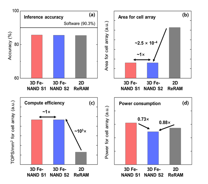
Fig. 4. Performance simulation; (a) Inference accuracy, (b) total cell array area, (c) Compute efficiency, (d) Power consumption.
In summary, we achieved the multi-level weight conductance states (≥ 256 levels/cell) of 3D FeNAND cells by engineering the interface trap density of gate stacks. The developed 3D FeNAND arrays demonstrated stable MAC operations with high accuracy (87.8%) and exhibited ultra-high compute efficiency, achieving a factor of 1,000x compared to 2D arrays. Our study provides an efficient method for developing ultra-high-density ACiM chips for edge computing with hyperscale AI models.
The Publication : Link
![[Summary] A Memristor-based In-Memory Computing SoC with Efficient Depthwise Convolution](https://mis-prod-koce-research-user-cdn-01-blob-ep.azureedge.net/web/blog/20260806/thumb_sEVmfv3K.20260806085519833.jpg)
![[Insights] Evolving Role of Emerging Memories in Next-Generation Computing](https://mis-prod-koce-research-user-cdn-01-blob-ep.azureedge.net/web/blog/20260806/thumb_NgJoNLYn.20260806080458980.jpg)
![[Summary] Electrical Characteristics of the 4F2 Vertical Gate (VG) DRAM integrated with Bit-Line Shielding (BLS) and Back Gate (BG) Transistor](https://mis-prod-koce-research-user-cdn-01-blob-ep.azureedge.net/web/blog/20260806/thumb_DOUurl5m.20260806080624234.png)