'%20fill='%23ea002c'/%3e%3cpath%20d='M31.44,109.48l7.92-9.71H33.72l-6.32,8.38h-.1V99.77H22.65v20.58h.28c2,0,4.4-.93,4.4-4.29v-4.73h.1l6.44,8.76h5.92Z'%20transform='translate(-5.29%20-72.33)'%20fill='%23ea002c'/%3e%3c/g%3e%3cg%3e%3cpath%20d='M39.63,77.72c-1.64.31-4.07,1.8-4.06,4.43,0,2.39,2,3.83,2,7a5.54,5.54,0,0,1-2.69,4.82c.57-.05,1.19-.08,1.87-.08a14.65,14.65,0,0,1,2.35.14l7.35-9A30.51,30.51,0,0,0,39.63,77.72Z'%20transform='translate(-5.29%20-72.33)'%20fill='%23ea002c'/%3e%3cpath%20d='M45.8,102.08c.93-1.44,1-3.74,1.12-6.07s.55-3.83,3.46-3.84c.65,0,1.26.09,2.38.09a17.2,17.2,0,0,0,8.8-2.46A30.54,30.54,0,0,0,46.41,85c-.41,1.18-3.67,10.23-3.92,11a11.32,11.32,0,0,1,1.32,1.93A21.12,21.12,0,0,1,45.8,102.08Z'%20transform='translate(-5.29%20-72.33)'%20fill='%23ea002c'/%3e%3cpath%20d='M30.28,94.69c-.38,0-.56-.25-.61-.68s-1.89-17.24-2.16-19.79c0-.37-.13-1-.13-1.3a.53.53,0,0,1,.55-.59c.87,0,5.62,1.11,10.66,4.64a5.37,5.37,0,0,0-4.07,5c0,2.77,2,4.29,2,7.07C36.54,93.59,31.35,94.69,30.28,94.69Z'%20transform='translate(-5.29%20-72.33)'%20fill='%23ff7a00'/%3e%3cpath%20d='M46.22,103.28a3.7,3.7,0,0,0,.23.51.52.52,0,0,0,.45.28,1.09,1.09,0,0,0,.42-.11l18.06-8.39c.33-.16,1-.45,1.18-.57a.56.56,0,0,0,.31-.49.58.58,0,0,0-.09-.3,18.5,18.5,0,0,0-4.25-3.76,19.07,19.07,0,0,1-9.63,2.78c-1.12,0-1.38-.08-2.14-.07-2.24,0-2.8,1-2.88,2.92,0,.37,0,.87,0,1.42C47.77,99.25,47.56,101.66,46.22,103.28Z'%20transform='translate(-5.29%20-72.33)'%20fill='%23ff7a00'/%3e%3c/g%3e%3cg%3e%3cpath%20d='M70.2,120.63c-1.7,4.61-3.89,5.2-5.78,5.2A5.55,5.55,0,0,1,62,125.3l.71-2.15a3.69,3.69,0,0,0,1.58.42c1.49,0,2.43-.84,3.26-3.44l-5.14-11.21a5.45,5.45,0,0,1,1.39-.21c1.65,0,2,1,2.43,2.06.36.85,2.7,6.51,2.7,6.51H69l2.72-8.36h2.81Z'%20transform='translate(-5.29%20-72.33)'%20fill='%23ff7a00'/%3e%3cpath%20d='M107.43,120.08l-3.93-5.72,3.85-5.6H104l-2.68,4.1-1.61-2.53c-.54-.83-1-1.66-2.25-1.63a2.46,2.46,0,0,0-.52,0,4.83,4.83,0,0,0-1.33.47c0,.06,1.89,2.68,3.65,5.22l-3.88,5.64h3.32l2.7-4.12,2.69,4.12Z'%20transform='translate(-5.29%20-72.33)'%20fill='%23ff7a00'/%3e%3cpath%20d='M76.84,112.6v7.49h2.81V112.3a3.79,3.79,0,0,1,2.26-1.09,2.16,2.16,0,0,1,2.2,2.41v6.47h2.81v-7.17a3.87,3.87,0,0,0-4.08-4.16,5.09,5.09,0,0,0-3.39,1.47A1.81,1.81,0,0,0,77.57,109a5.79,5.79,0,0,0-1,.14A14.85,14.85,0,0,1,76.84,112.6Z'%20transform='translate(-5.29%20-72.33)'%20fill='%23ff7a00'/%3e%3cg%3e%3cpath%20d='M93.2,105.54a1.74,1.74,0,1,1-1.74-1.69A1.71,1.71,0,0,1,93.2,105.54Z'%20transform='translate(-5.29%20-72.33)'%20fill='%23ff7a00'/%3e%3crect%20x='84.78'%20y='36.59'%20width='2.79'%20height='11.16'%20fill='%23ff7a00'/%3e%3c/g%3e%3cpath%20d='M53.44,110.2a5.74,5.74,0,0,1,3.62-1.49c2.19,0,3.8,1.14,3.8,3.91v7.47H57.94v-6.67a2,2,0,0,0-2-2.18,4.24,4.24,0,0,0-2.54,1.21v7.64h-2.9v-17h.62a2.22,2.22,0,0,1,2.28,2.35Z'%20transform='translate(-5.29%20-72.33)'%20fill='%23ff7a00'/%3e%3c/g%3e%3c/g%3e%3c/svg%3e)
[Summary] Achieving Outstanding Endurance (> 107) in Large-Array Two-Deck 16 nm SOM through Process, Structure, and Design Strategies for Emerging SCM Applications
This study was presented at the 2025 IEEE Symposium on VLSI Technology and Circuits (VLSI 2025), held June 8–12, 2025, in Kyoto, Japan. Selector-only memory (SOM) has emerged as one of the most promising storage-class memory (SCM) candidates beyond 3D XPoint, offering clear advantages in scalability, process complexity, and latency. With latency shorter than 100 ns and excellent endurance characteristics, SOM holds significant potential for applications in compute express link (CXL) environments. To achieve near-DRAM performance, endurance exceeding 107 cycles is critical for SCM.
In this study, we successfully integrated a 16 nm half-pitch SOM with a two-deck architecture, configured into a 4k × 4k array mat. Through process, structure, and design approaches, we achieved endurance exceeding 107 cycles, effectively addressing key challenges associated with large-scale SOM arrays and their integration.
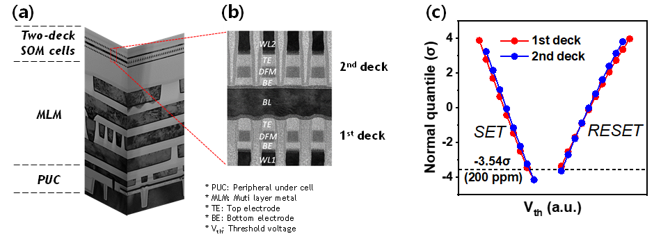
Fig. 1(a) and (b) shows TEM images of a two-deck 16 nm half-pitch SOM cell array, with the 1st and 2nd decks sharing a common BL and identical cell structures. Robust read window margin (RWM) characteristics for both decks, with no degradation observed in the tail properties of the SET/RESET distribution, are demonstrated in Fig. 1(c).
Fig. 1. (a) Cross-sectional TEM image of a 16 nm half-pitch, two-deck cross-point SOM featuring PUC architecture. (b) Array of two-deck SOM cells. (c) SET/RESET Vth distributions in 1st deck and 2nd deck SOM arrays.
Fig. 2(a) shows the cycling endurance trend of our dual-functional material (DFM) system with varying As concentration. DFT simulations suggest that increased As content reduces atomic mobility and stabilizes the amorphous structure, enhancing endurance. Based on this, we optimized the As concentration to balance endurance and electrical performance. We also found that oxidation-induced encapsulation deformation degrades endurance. To prevent this, we developed an enhanced encapsulation process (EEP), which improved endurance by a factor of 2.47, as shown in Fig. 2(b). Further process optimizations—including refined etch conditions, improved array encapsulation, and DFM composition tuning—yielded additional endurance gains, as shown in Fig. 2(c).
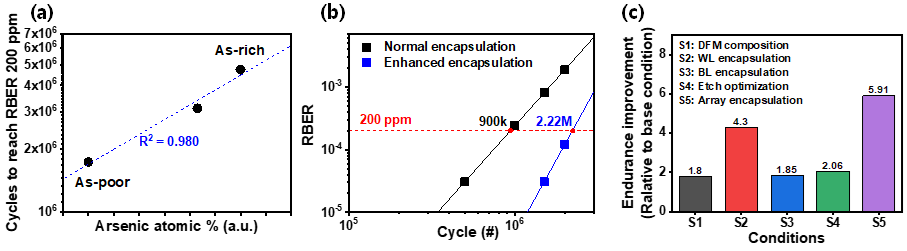
Fig. 2. (a) Endurance characteristics as a function of As concentration in DFM. (b) Cycle vs. RBER showing improved endurance with enhanced encapsulation compared to the normal encapsulation process. (c) Endurance improvement relative to the base condition for S1, S2, S3, S4, and S5.
To suppress the spike current in the zone NEAR, we optimized the cell stack resistance. As shown in Fig. 3(a), our cell stack incorporates electrodes and resistance layers (RLs) capable of providing additional resistance. Notably, the RL exhibited up to approximately a 7-fold change in resistivity depending on the process conditions (Fig. 3(b)), with additional tunability achieved through thickness adjustment (Fig. 3(c)).
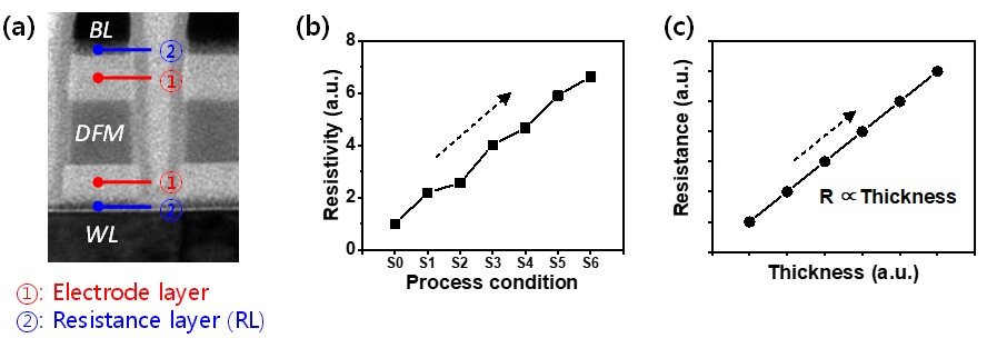
Fig. 3. (a) Electrode and resistance layers for cell stack resistance. (b) Resistivity of the resistance layer (RL) as a function of process conditions. (c) Resistance as a function of RL thickness.
We implemented a local X switch gate voltage (VLXG) control scheme to suppress spike current in the zone NEAR during write/read operations (Fig. 4(a)). Additionally, SOM Vth scaling reduced operating voltage, lowering spike charge and improving power efficiency (Fig. 4(b)). As a result, 2R1W power consumption was reduced by 47% in Stage 2 compared to Stage 1 (Fig. 4(c)).
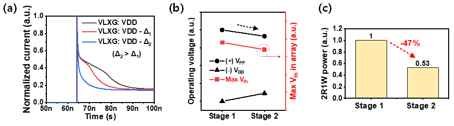
Fig. 4. (a) Time vs. cell current as a function of VLXG, simulated for the zone NEAR. (b) Reduction in operating voltage achieved through Vth scaling of SOM. (c) Comparison of two read, one write (2R1W) power consumption between Stage 1 and Stage 2.
Fig. 5 summarizes the key factors and processes that contribute to achieving endurance characteristics exceeding 107 cycles. In summary, this study successfully demonstrated, for the first time, a 16 nm half-pitch SOM with a two-deck architecture, achieving endurance beyond 107 cycles. The approaches employed here are expected to play a significant role in establishing SOM as a robust candidate for emerging SCM applications.
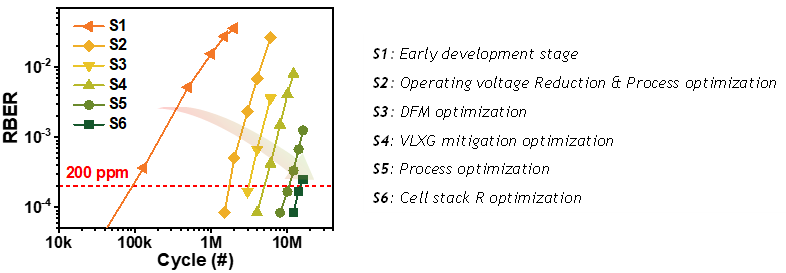
Fig. 5. Cycle vs. RBER showing endurance improvements from different factors.
The Publication : Link

![[Summary] A Memristor-based In-Memory Computing SoC with Efficient Depthwise Convolution](https://mis-prod-koce-research-user-cdn-01-blob-ep.azureedge.net/web/blog/20260806/thumb_sEVmfv3K.20260806085519833.jpg)
![[Insights] Evolving Role of Emerging Memories in Next-Generation Computing](https://mis-prod-koce-research-user-cdn-01-blob-ep.azureedge.net/web/blog/20260806/thumb_NgJoNLYn.20260806080458980.jpg)
![[Summary] Electrical Characteristics of the 4F2 Vertical Gate (VG) DRAM integrated with Bit-Line Shielding (BLS) and Back Gate (BG) Transistor](https://mis-prod-koce-research-user-cdn-01-blob-ep.azureedge.net/web/blog/20260806/thumb_DOUurl5m.20260806080624234.png)