'%20fill='%23ea002c'/%3e%3cpath%20d='M31.44,109.48l7.92-9.71H33.72l-6.32,8.38h-.1V99.77H22.65v20.58h.28c2,0,4.4-.93,4.4-4.29v-4.73h.1l6.44,8.76h5.92Z'%20transform='translate(-5.29%20-72.33)'%20fill='%23ea002c'/%3e%3c/g%3e%3cg%3e%3cpath%20d='M39.63,77.72c-1.64.31-4.07,1.8-4.06,4.43,0,2.39,2,3.83,2,7a5.54,5.54,0,0,1-2.69,4.82c.57-.05,1.19-.08,1.87-.08a14.65,14.65,0,0,1,2.35.14l7.35-9A30.51,30.51,0,0,0,39.63,77.72Z'%20transform='translate(-5.29%20-72.33)'%20fill='%23ea002c'/%3e%3cpath%20d='M45.8,102.08c.93-1.44,1-3.74,1.12-6.07s.55-3.83,3.46-3.84c.65,0,1.26.09,2.38.09a17.2,17.2,0,0,0,8.8-2.46A30.54,30.54,0,0,0,46.41,85c-.41,1.18-3.67,10.23-3.92,11a11.32,11.32,0,0,1,1.32,1.93A21.12,21.12,0,0,1,45.8,102.08Z'%20transform='translate(-5.29%20-72.33)'%20fill='%23ea002c'/%3e%3cpath%20d='M30.28,94.69c-.38,0-.56-.25-.61-.68s-1.89-17.24-2.16-19.79c0-.37-.13-1-.13-1.3a.53.53,0,0,1,.55-.59c.87,0,5.62,1.11,10.66,4.64a5.37,5.37,0,0,0-4.07,5c0,2.77,2,4.29,2,7.07C36.54,93.59,31.35,94.69,30.28,94.69Z'%20transform='translate(-5.29%20-72.33)'%20fill='%23ff7a00'/%3e%3cpath%20d='M46.22,103.28a3.7,3.7,0,0,0,.23.51.52.52,0,0,0,.45.28,1.09,1.09,0,0,0,.42-.11l18.06-8.39c.33-.16,1-.45,1.18-.57a.56.56,0,0,0,.31-.49.58.58,0,0,0-.09-.3,18.5,18.5,0,0,0-4.25-3.76,19.07,19.07,0,0,1-9.63,2.78c-1.12,0-1.38-.08-2.14-.07-2.24,0-2.8,1-2.88,2.92,0,.37,0,.87,0,1.42C47.77,99.25,47.56,101.66,46.22,103.28Z'%20transform='translate(-5.29%20-72.33)'%20fill='%23ff7a00'/%3e%3c/g%3e%3cg%3e%3cpath%20d='M70.2,120.63c-1.7,4.61-3.89,5.2-5.78,5.2A5.55,5.55,0,0,1,62,125.3l.71-2.15a3.69,3.69,0,0,0,1.58.42c1.49,0,2.43-.84,3.26-3.44l-5.14-11.21a5.45,5.45,0,0,1,1.39-.21c1.65,0,2,1,2.43,2.06.36.85,2.7,6.51,2.7,6.51H69l2.72-8.36h2.81Z'%20transform='translate(-5.29%20-72.33)'%20fill='%23ff7a00'/%3e%3cpath%20d='M107.43,120.08l-3.93-5.72,3.85-5.6H104l-2.68,4.1-1.61-2.53c-.54-.83-1-1.66-2.25-1.63a2.46,2.46,0,0,0-.52,0,4.83,4.83,0,0,0-1.33.47c0,.06,1.89,2.68,3.65,5.22l-3.88,5.64h3.32l2.7-4.12,2.69,4.12Z'%20transform='translate(-5.29%20-72.33)'%20fill='%23ff7a00'/%3e%3cpath%20d='M76.84,112.6v7.49h2.81V112.3a3.79,3.79,0,0,1,2.26-1.09,2.16,2.16,0,0,1,2.2,2.41v6.47h2.81v-7.17a3.87,3.87,0,0,0-4.08-4.16,5.09,5.09,0,0,0-3.39,1.47A1.81,1.81,0,0,0,77.57,109a5.79,5.79,0,0,0-1,.14A14.85,14.85,0,0,1,76.84,112.6Z'%20transform='translate(-5.29%20-72.33)'%20fill='%23ff7a00'/%3e%3cg%3e%3cpath%20d='M93.2,105.54a1.74,1.74,0,1,1-1.74-1.69A1.71,1.71,0,0,1,93.2,105.54Z'%20transform='translate(-5.29%20-72.33)'%20fill='%23ff7a00'/%3e%3crect%20x='84.78'%20y='36.59'%20width='2.79'%20height='11.16'%20fill='%23ff7a00'/%3e%3c/g%3e%3cpath%20d='M53.44,110.2a5.74,5.74,0,0,1,3.62-1.49c2.19,0,3.8,1.14,3.8,3.91v7.47H57.94v-6.67a2,2,0,0,0-2-2.18,4.24,4.24,0,0,0-2.54,1.21v7.64h-2.9v-17h.62a2.22,2.22,0,0,1,2.28,2.35Z'%20transform='translate(-5.29%20-72.33)'%20fill='%23ff7a00'/%3e%3c/g%3e%3c/g%3e%3c/svg%3e)
[Summary] Demonstration of Ultra-thin Ferroelectric/dielectric and Anti-ferroelectric/dielectric Bilayers for Future DRAM Cell Capacitors
One of the critical challenges as DRAM cell scaling continues is that DRAM cell capacitances are decreased In order to meet criteria for future DRAM cell capacitors, it is imperative to develop dielectric materials having a higher dielectric constant (k) in an ultra-thin physical thickness (< 6 nm) with low leakage currents.
In this study, we optimized ultra-thin ferroelectric (FE)/dielectric (DE) and anti-ferroelectric (AFE)/DE bilayers for applications in DRAM cell capacitors (Fig. 1). We further demonstrated their real operation in 1T1C DRAM cells in 12-inch wafers using the state-of-the-art 1X nm DRAM technology.
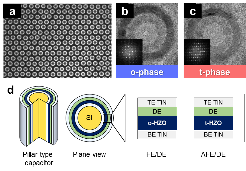
Fig. 1. (a) TEM image of pillar-type capacitor arrays. TEM images of (b) o-phase rich and (c) t-phase rich HZO thin-films. (d) Schematic illustration of FE/DE and AFE/DE capacitors.
We controlled the capacitance ratios of FE/DE (C[FE]/C[DE]) and AFE/DE (C[AFE]/C[DE]) bilayers to optimize electrical properties, in terms of equivalent oxide thickness (EOT) and remnant charges (Qrem) at 0.6 V. The decrease in the EOT of FE/DE capacitors is accompanied with the rapid increase in Qrem. On the other hand, the AFE/DE capacitors exhibited very slow increase in Qrem as decreasing EOT values, due to the small Qrem and higher Vc of AFE-like t-phase HZO than those of FE o-phase HZO.
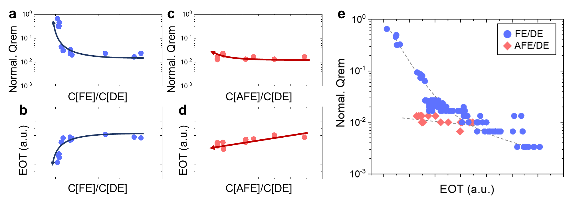
Fig. 2. Qrem and EOT as a function of (a,b) C[FE]/C[DE] and (c,d) C[AFE]/C[DE]. (e) Trend of normalized Qrem and EOT for various capacitors.
In addition, we demonstrated 1X nm DRAM operations of AFE/DE and FE/DE capacitors using a typical DRAM write recovery time (tWR) evaluation method at hot (95°C) and cold (–10°C) temperature (Fig. 3). Even though the capacitors have similar BV and EOT values, the AFE/DE capacitors showed significantly fewer write failures than the FE/DE capacitors. This tendency is because large amounts of Qrem in the FE/DE capacitors acts as opposite polarities during write operation and hinders subsequent DRAM operations.
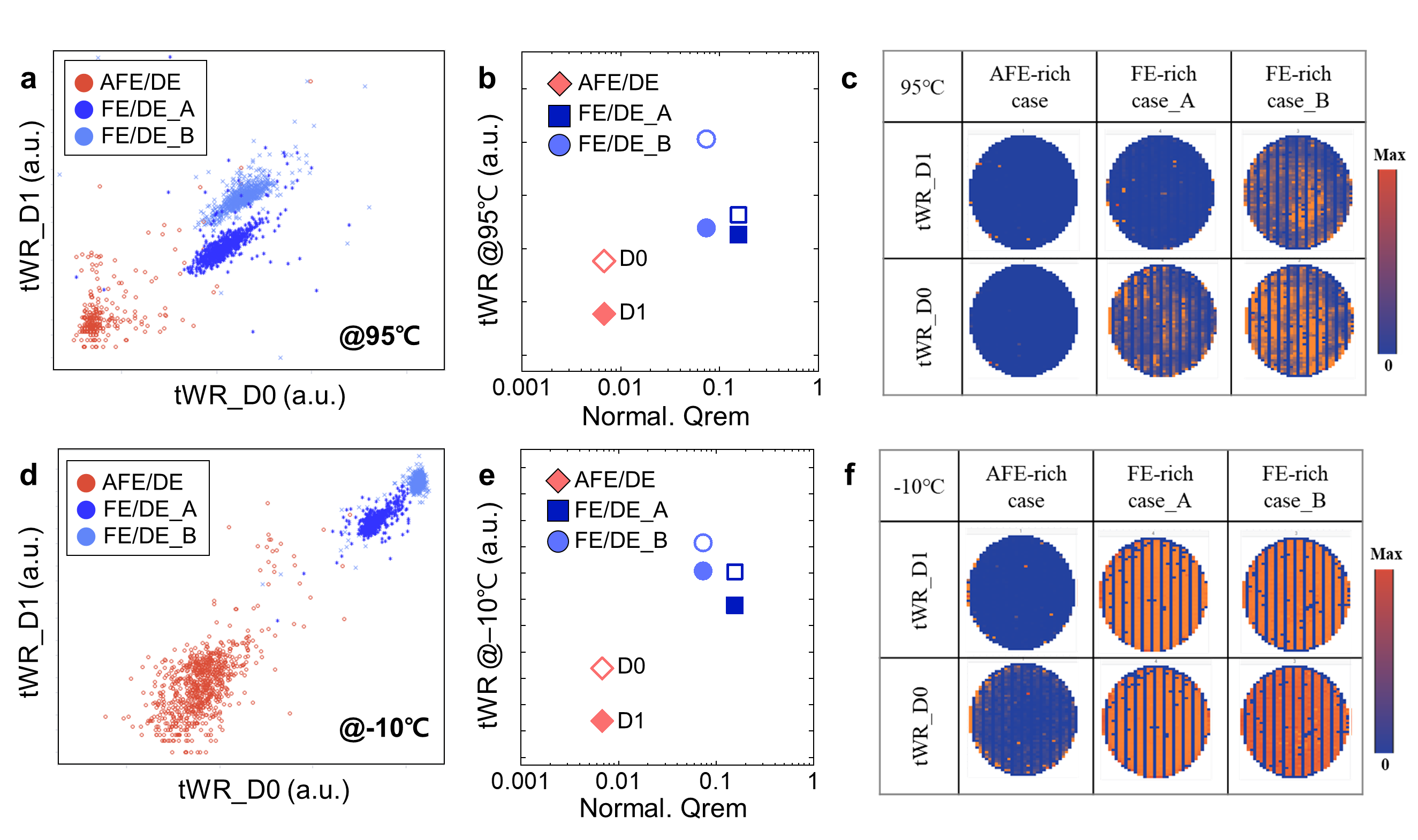
Fig. 3. DRAM tWR results at (a-c) 95℃ and (d-f) –10℃. (a,d) Scatter plots for fail bits, (b,e) Normalized Qrem versus tWR, and (c,f) 12-inch wafer maps for fail bits.
In summary, we investigated the electrical properties of FE/DE and AFE/DE bilayers as a function of capacitance ratios, and demonstrated their real operation in 1X nm DRAM cells. Our study revealed that the strict control of Qrem is necessary to stable DRAM operations, thereby indicating that AFE/DE layers are more favorable than FE/DE layers for use as DRAM cell capacitors.
The publication: Link

![[Summary] A Memristor-based In-Memory Computing SoC with Efficient Depthwise Convolution](https://mis-prod-koce-research-user-cdn-01-blob-ep.azureedge.net/web/blog/20260806/thumb_sEVmfv3K.20260806085519833.jpg)
![[Insights] Evolving Role of Emerging Memories in Next-Generation Computing](https://mis-prod-koce-research-user-cdn-01-blob-ep.azureedge.net/web/blog/20260806/thumb_NgJoNLYn.20260806080458980.jpg)
![[Summary] Electrical Characteristics of the 4F2 Vertical Gate (VG) DRAM integrated with Bit-Line Shielding (BLS) and Back Gate (BG) Transistor](https://mis-prod-koce-research-user-cdn-01-blob-ep.azureedge.net/web/blog/20260806/thumb_DOUurl5m.20260806080624234.png)