'%20fill='%23ea002c'/%3e%3cpath%20d='M31.44,109.48l7.92-9.71H33.72l-6.32,8.38h-.1V99.77H22.65v20.58h.28c2,0,4.4-.93,4.4-4.29v-4.73h.1l6.44,8.76h5.92Z'%20transform='translate(-5.29%20-72.33)'%20fill='%23ea002c'/%3e%3c/g%3e%3cg%3e%3cpath%20d='M39.63,77.72c-1.64.31-4.07,1.8-4.06,4.43,0,2.39,2,3.83,2,7a5.54,5.54,0,0,1-2.69,4.82c.57-.05,1.19-.08,1.87-.08a14.65,14.65,0,0,1,2.35.14l7.35-9A30.51,30.51,0,0,0,39.63,77.72Z'%20transform='translate(-5.29%20-72.33)'%20fill='%23ea002c'/%3e%3cpath%20d='M45.8,102.08c.93-1.44,1-3.74,1.12-6.07s.55-3.83,3.46-3.84c.65,0,1.26.09,2.38.09a17.2,17.2,0,0,0,8.8-2.46A30.54,30.54,0,0,0,46.41,85c-.41,1.18-3.67,10.23-3.92,11a11.32,11.32,0,0,1,1.32,1.93A21.12,21.12,0,0,1,45.8,102.08Z'%20transform='translate(-5.29%20-72.33)'%20fill='%23ea002c'/%3e%3cpath%20d='M30.28,94.69c-.38,0-.56-.25-.61-.68s-1.89-17.24-2.16-19.79c0-.37-.13-1-.13-1.3a.53.53,0,0,1,.55-.59c.87,0,5.62,1.11,10.66,4.64a5.37,5.37,0,0,0-4.07,5c0,2.77,2,4.29,2,7.07C36.54,93.59,31.35,94.69,30.28,94.69Z'%20transform='translate(-5.29%20-72.33)'%20fill='%23ff7a00'/%3e%3cpath%20d='M46.22,103.28a3.7,3.7,0,0,0,.23.51.52.52,0,0,0,.45.28,1.09,1.09,0,0,0,.42-.11l18.06-8.39c.33-.16,1-.45,1.18-.57a.56.56,0,0,0,.31-.49.58.58,0,0,0-.09-.3,18.5,18.5,0,0,0-4.25-3.76,19.07,19.07,0,0,1-9.63,2.78c-1.12,0-1.38-.08-2.14-.07-2.24,0-2.8,1-2.88,2.92,0,.37,0,.87,0,1.42C47.77,99.25,47.56,101.66,46.22,103.28Z'%20transform='translate(-5.29%20-72.33)'%20fill='%23ff7a00'/%3e%3c/g%3e%3cg%3e%3cpath%20d='M70.2,120.63c-1.7,4.61-3.89,5.2-5.78,5.2A5.55,5.55,0,0,1,62,125.3l.71-2.15a3.69,3.69,0,0,0,1.58.42c1.49,0,2.43-.84,3.26-3.44l-5.14-11.21a5.45,5.45,0,0,1,1.39-.21c1.65,0,2,1,2.43,2.06.36.85,2.7,6.51,2.7,6.51H69l2.72-8.36h2.81Z'%20transform='translate(-5.29%20-72.33)'%20fill='%23ff7a00'/%3e%3cpath%20d='M107.43,120.08l-3.93-5.72,3.85-5.6H104l-2.68,4.1-1.61-2.53c-.54-.83-1-1.66-2.25-1.63a2.46,2.46,0,0,0-.52,0,4.83,4.83,0,0,0-1.33.47c0,.06,1.89,2.68,3.65,5.22l-3.88,5.64h3.32l2.7-4.12,2.69,4.12Z'%20transform='translate(-5.29%20-72.33)'%20fill='%23ff7a00'/%3e%3cpath%20d='M76.84,112.6v7.49h2.81V112.3a3.79,3.79,0,0,1,2.26-1.09,2.16,2.16,0,0,1,2.2,2.41v6.47h2.81v-7.17a3.87,3.87,0,0,0-4.08-4.16,5.09,5.09,0,0,0-3.39,1.47A1.81,1.81,0,0,0,77.57,109a5.79,5.79,0,0,0-1,.14A14.85,14.85,0,0,1,76.84,112.6Z'%20transform='translate(-5.29%20-72.33)'%20fill='%23ff7a00'/%3e%3cg%3e%3cpath%20d='M93.2,105.54a1.74,1.74,0,1,1-1.74-1.69A1.71,1.71,0,0,1,93.2,105.54Z'%20transform='translate(-5.29%20-72.33)'%20fill='%23ff7a00'/%3e%3crect%20x='84.78'%20y='36.59'%20width='2.79'%20height='11.16'%20fill='%23ff7a00'/%3e%3c/g%3e%3cpath%20d='M53.44,110.2a5.74,5.74,0,0,1,3.62-1.49c2.19,0,3.8,1.14,3.8,3.91v7.47H57.94v-6.67a2,2,0,0,0-2-2.18,4.24,4.24,0,0,0-2.54,1.21v7.64h-2.9v-17h.62a2.22,2.22,0,0,1,2.28,2.35Z'%20transform='translate(-5.29%20-72.33)'%20fill='%23ff7a00'/%3e%3c/g%3e%3c/g%3e%3c/svg%3e)
[Invited Insights] Demonstration of thin film process for chalcogenide-based selector-only-memory technology
The European Phase-Change and Ovonic Symposium (EPCOS) took place in Leipzig, Germany in September 2024. Historically, EPCOS has served as a premier forum for academia and industry to share cutting-edge scientific and technological advancements in phase-change and Ovonic materials, particularly for applications in data storage, memory devices, and emerging fields. This year’s three-day event featured 10 single sessions, with 15 invited talks and 24 contributed presentations from both academic and industry experts.
The first and second sessions focused on “OTS-SOM” (Ovonic Threshold Switch - Selector-Only Memory), drawing significant attention from attendees. The Ovonic Threshold Switch (OTS), commonly used as a selector device for phase-change memory (PCM), has long been studied. However, researchers from IMEC reported a polarity-dependent shift in threshold voltage (Vth), which presents a great challenge and opportunity as a new memory, selector-only memory (SOM); This memory effect, originating from the SOM device, could significantly reduce the complexity of integrating PCM with OTS and potentially increase the operation speed to below 50 ns. Additionally, by incorporating a vertical X-Point architecture, the simplified SOM device could greatly enhance memory density.
We presented the development of an atomic layer deposition (ALD) process for GeSe-based chalcogenide thin films. The ALD process offers significant advantages, particularly its ability to grow conformal thin films with precise thickness control. Advancements in ALD techniques for Se-based thin films also support the development of SOM devices, enabling high-density integration through the memory-selector duality within a 3D structure. This work was result of the 2-year research project supported by SK hynix Inc.
In this work, thermal ALD process of GeSe thin film at high temperature showed a growth rate of 0.11, 0.11, and 0.02 nm/cycle at 190, 220, and 250 ℃, respectively. X-ray fluorescence analysis also showed the linear growth of the layer density as the number of cycle increased. In the case of the 220℃ process (Figure 1a), a linear increase in layer density according to the cycle and a composition close to Ge:Se=0.6:0.4 were confirmed. The cross-sectional scanning electron microscopic image of the film deposited for 200 cycles at 220℃ (Figure 1b) shows the uniform thin film. As shown in Fig. 1c, ALD process of GeSe can grow the conformal thin film on a trench patterned wafer with an aspect ratio of 32:1. This result indicates a step coverage of about 90%. Fig. 1d shows the current-voltage curve of W/GeSe/W device, where threshold switching was observed above 5V of operation voltage. We also presented the possibility of ternary GeSeIn film by adopting the GeSe buffer layer and super-cycle of GeSe and InSe ALD, respectively. We believe that this work paves the way of development of vertical SOM architecture of dual functional devices with high-quality GeSe-based chalcogenide thin films.
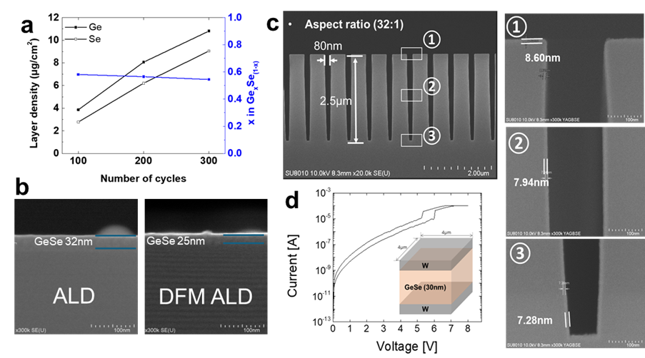
Figure. 1 a) Layer density and composition of GeSe thin film as a function of ALD-cycles grown at 220℃, b) cross-sectional SEM image of GeSe thin film grown at 220℃, c) cross-sectional SEM images of GeSe thin film grown on trench pattern, d) I-V curve of W/GeSe/W device.
This study included the participation of researcher from SK hynix inc., that remains committed to collaborating with academic institutions in the pursuit of groundbreaking future memory semiconductor research.

![[Summary] A Memristor-based In-Memory Computing SoC with Efficient Depthwise Convolution](https://mis-prod-koce-research-user-cdn-01-blob-ep.azureedge.net/web/blog/20260806/thumb_sEVmfv3K.20260806085519833.jpg)
![[Insights] Evolving Role of Emerging Memories in Next-Generation Computing](https://mis-prod-koce-research-user-cdn-01-blob-ep.azureedge.net/web/blog/20260806/thumb_NgJoNLYn.20260806080458980.jpg)
![[Summary] Electrical Characteristics of the 4F2 Vertical Gate (VG) DRAM integrated with Bit-Line Shielding (BLS) and Back Gate (BG) Transistor](https://mis-prod-koce-research-user-cdn-01-blob-ep.azureedge.net/web/blog/20260806/thumb_DOUurl5m.20260806080624234.png)